Electrical ratings
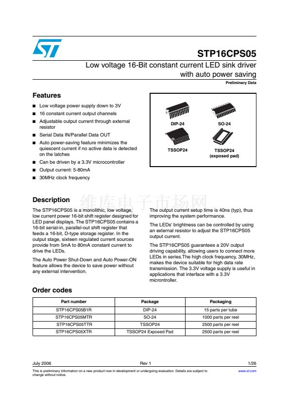
STP16CPS05
2
2.1
Electrical ratings
Absolute maximum ratings
Stressing the device above the rating listed in the 鈥淎bsolute Maximum Ratings鈥?table may
cause permanent damage to the device. These are stress ratings only and operation of the
device at these or any other conditions above those indicated in the Operating sections of
this specification is not implied. Exposure to Absolute Maximum Rating conditions for
extended periods may affect device reliability. Refer also to the STMicroelectronics SURE
Program and other relevant quality documents.
Table 3.
Symbol
V
DD
V
O
I
O
V
I
I
GND
f
CLK
Supply voltage
Output voltage
Output current
Input voltage
GND terminal current
Clock frequency
Absolute maximum ratings
Parameter
Value
0 to 7
-0.5 to 20
80
-0.4 to V
DD
+0.4
1300
30
Unit
V
V
mA
V
mA
MHz
2.2
Thermal data
Table 4.
Symbol
T
OPR
T
STG
Thermal data
Parameter
Operating temperature range
Storage temperature range
DIP-24
TSSOP24
Value
-40 to +125
-55 to +150
60
85
37.5
75
Unit
掳C
掳C
掳C/W
掳C/W
掳C/W
掳C/W
R
thJC
Thermal resistance junction-case
TSSOP24
(1)
Exposed Pad
SO-24
1. The exposed pad should be soldered directly to the PCB to realize the thermal benefits.
4/26


 1
1
 2
2
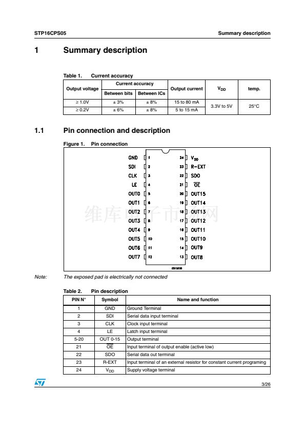 3
3
 4
4
 5
5
 6
6
 7
7
 8
8
 9
9
 10
10
 11
11
 12
12
 13
13
 14
14
 15
15
 16
16
 17
17
 18
18
 19
19
 20
20
 21
21
 22
22
 23
23
 24
24
 25
25
 26
26
