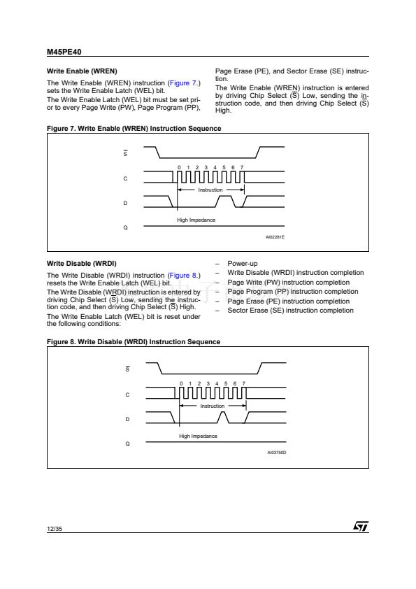
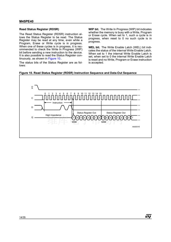
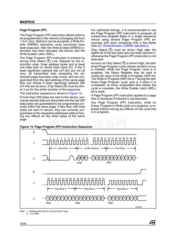
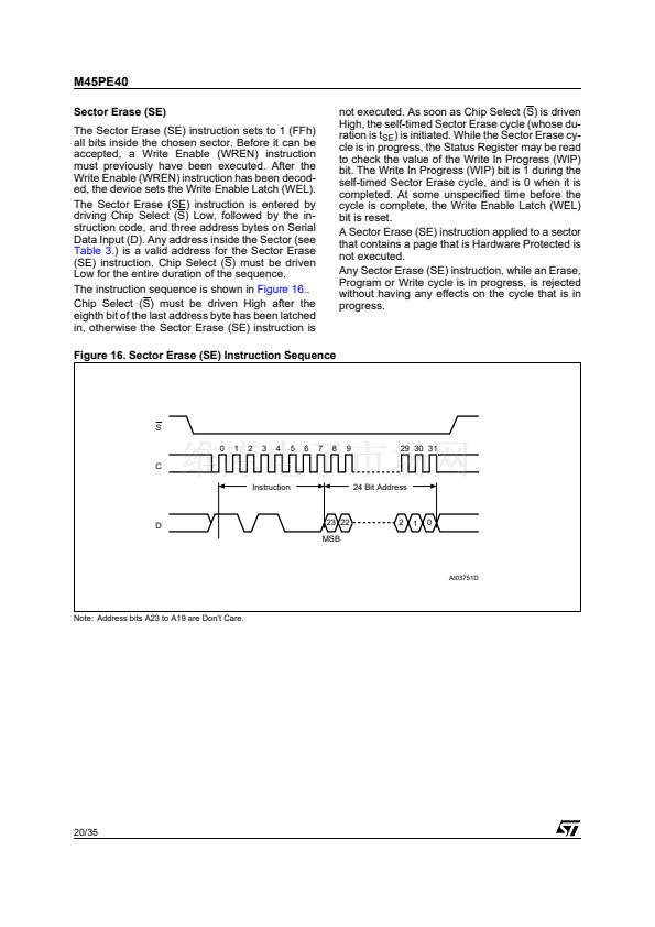
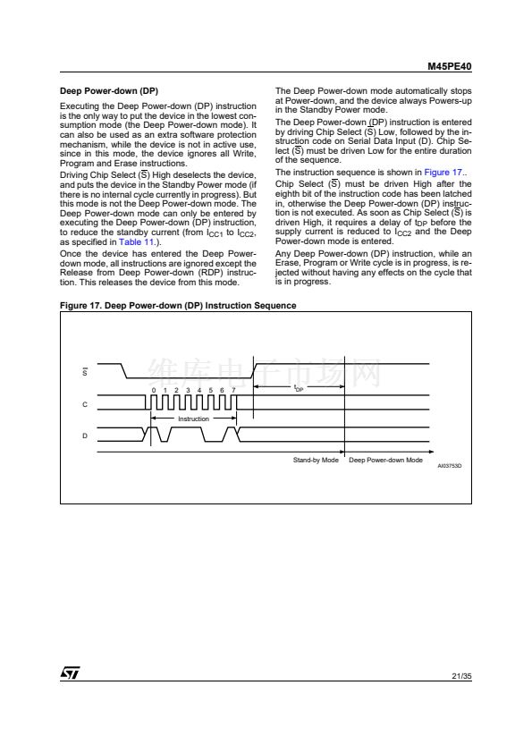
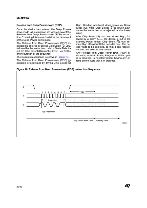
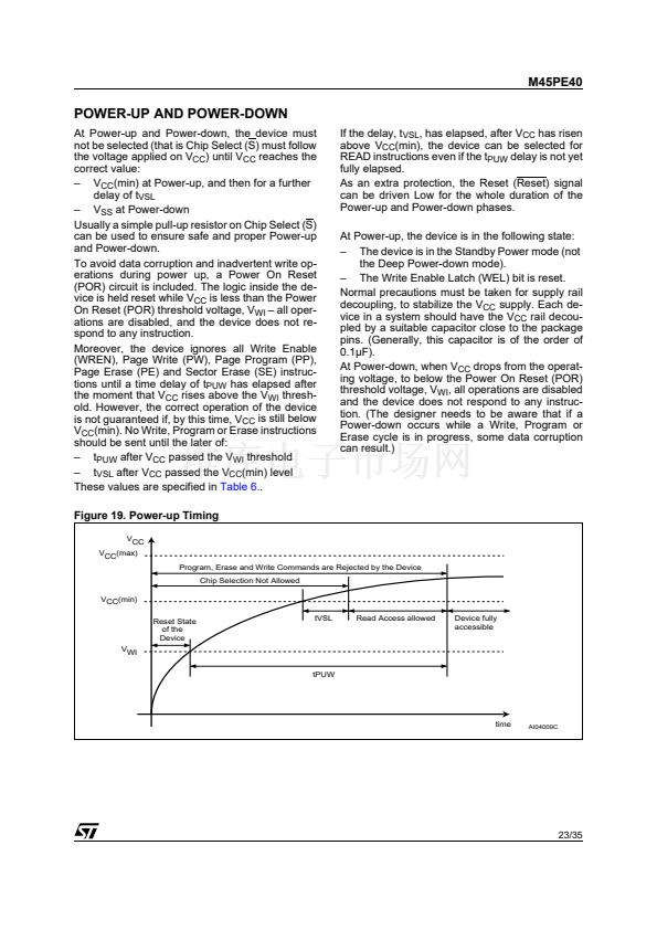
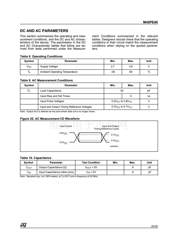
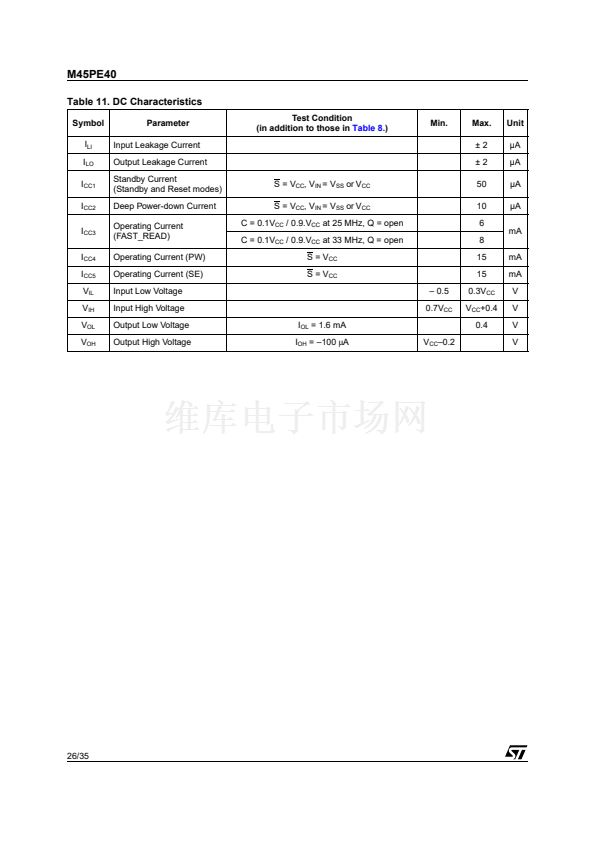
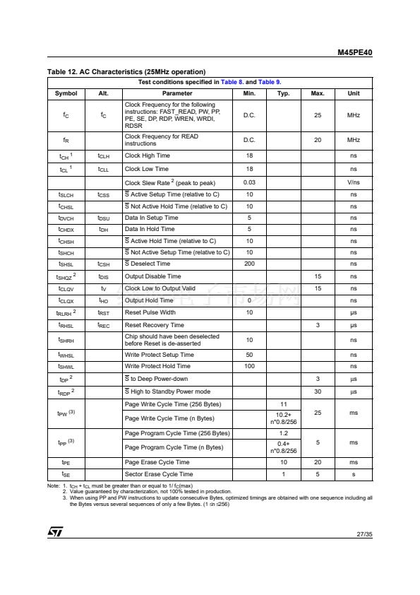
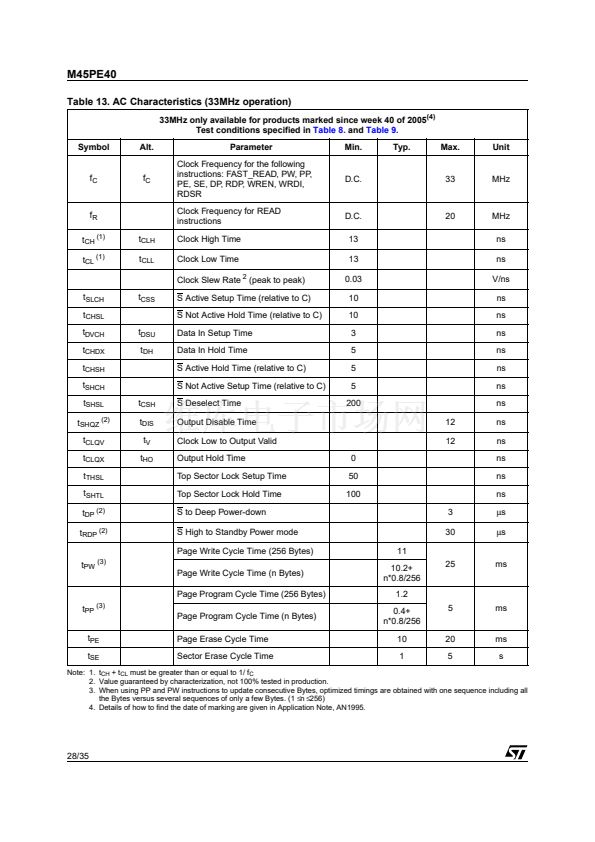
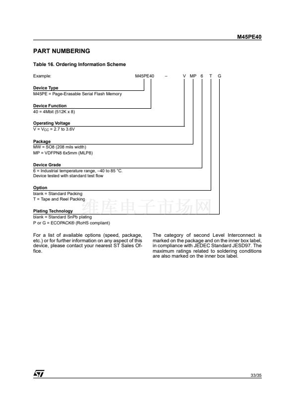
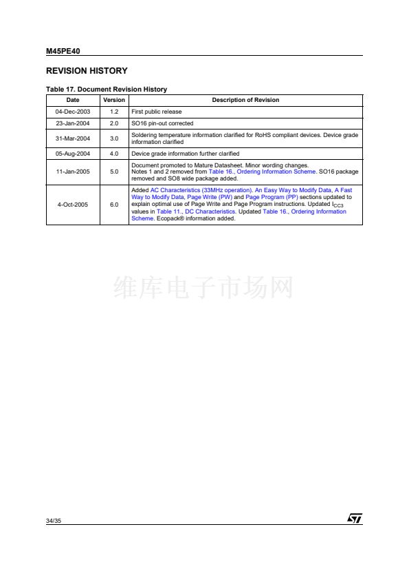
M45PE40
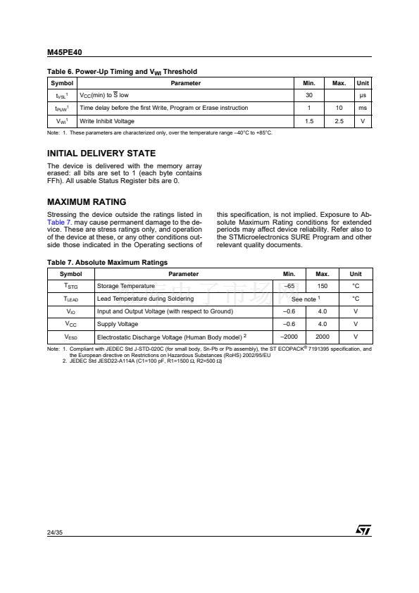
Table 6. Power-Up Timing and V
WI
Threshold
Symbol
t
VSL1
t
PUW1
V
WI1
V
CC
(min) to S low
Time delay before the first Write, Program or Erase instruction
Write Inhibit Voltage
Parameter
Min.
30
1
1.5
10
2.5
Max.
Unit
碌s
ms
V
Note: 1. These parameters are characterized only, over the temperature range 鈥?0掳C to +85掳C.
INITIAL DELIVERY STATE
The device is delivered with the memory array
erased: all bits are set to 1 (each byte contains
FFh). All usable Status Register bits are 0.
MAXIMUM RATING
Stressing the device outside the ratings listed in
Table 7.
may cause permanent damage to the de-
vice. These are stress ratings only, and operation
of the device at these, or any other conditions out-
side those indicated in the Operating sections of
Table 7. Absolute Maximum Ratings
Symbol
T
STG
T
LEAD
V
IO
V
CC
V
ESD
Storage Temperature
Lead Temperature during Soldering
Input and Output Voltage (with respect to Ground)
Supply Voltage
Electrostatic Discharge Voltage (Human Body model)
2
Parameter
Min.
鈥?5
Max.
150
Unit
掳C
掳C
V
V
V
this specification, is not implied. Exposure to Ab-
solute Maximum Rating conditions for extended
periods may affect device reliability. Refer also to
the STMicroelectronics SURE Program and other
relevant quality documents.
See note
1
鈥?.6
鈥?.6
鈥?000
4.0
4.0
2000
Note: 1. Compliant with JEDEC Std J-STD-020C (for small body, Sn-Pb or Pb assembly), the ST ECOPACK
庐
7191395 specification, and
the European directive on Restrictions on Hazardous Substances (RoHS) 2002/95/EU
2. JEDEC Std JESD22-A114A (C1=100 pF, R1=1500
鈩?
R2=500
鈩?
24/35


 1
1
 2
2
 3
3
 4
4
 5
5
 6
6
 7
7
 8
8
 9
9
 10
10
 11
11
 12
12
 13
13
 14
14
 15
15
 16
16
 17
17
 18
18
 19
19
 20
20
 21
21
 22
22
 23
23
 24
24
 25
25
 26
26
 27
27
 28
28
 29
29
 30
30
 31
31
 32
32
 33
33
 34
34
 35
35
