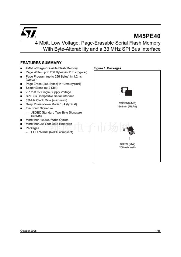
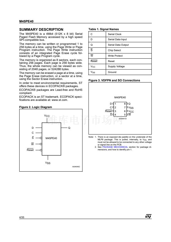
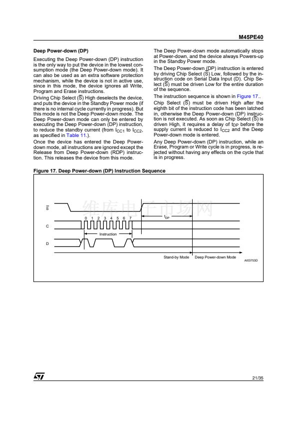
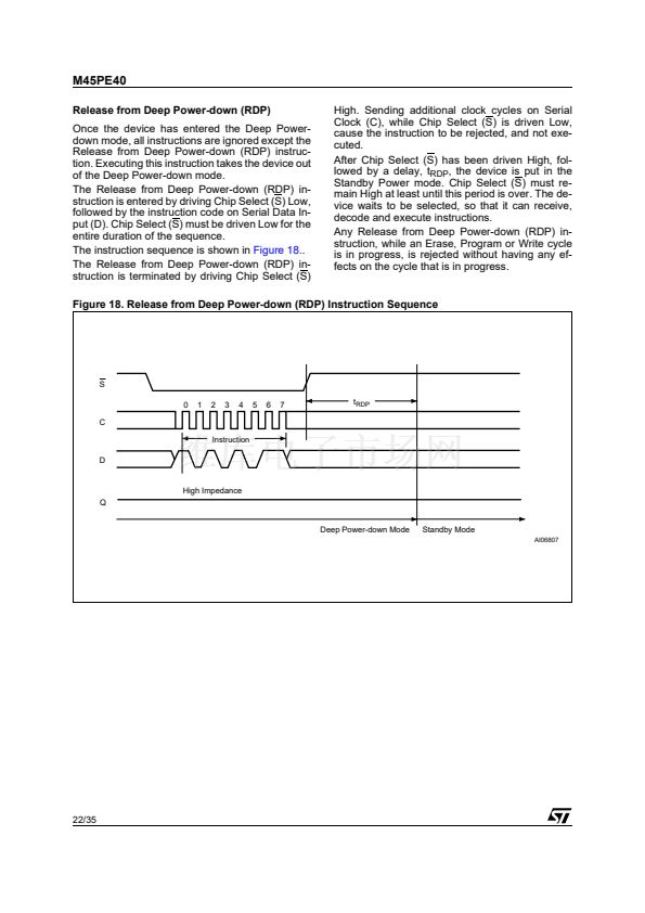
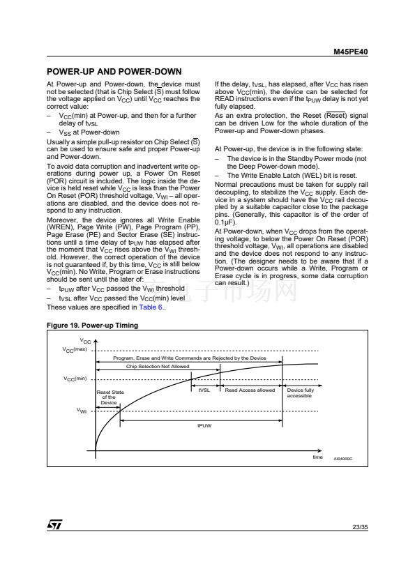
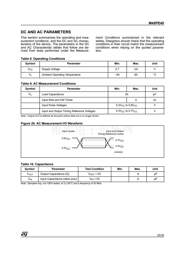
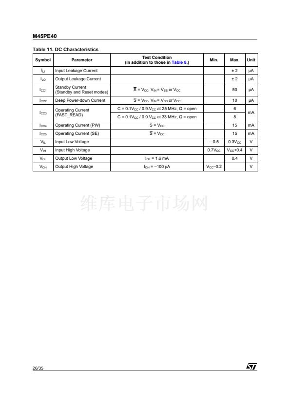
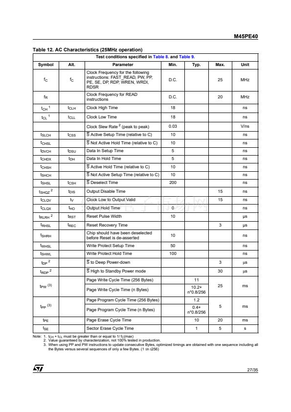
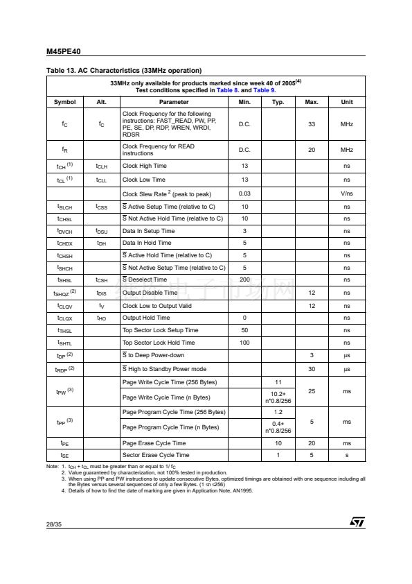
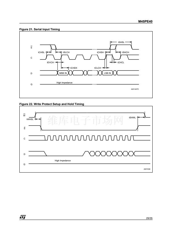
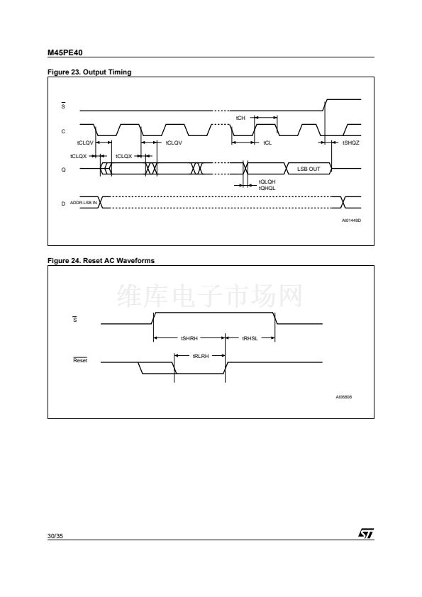
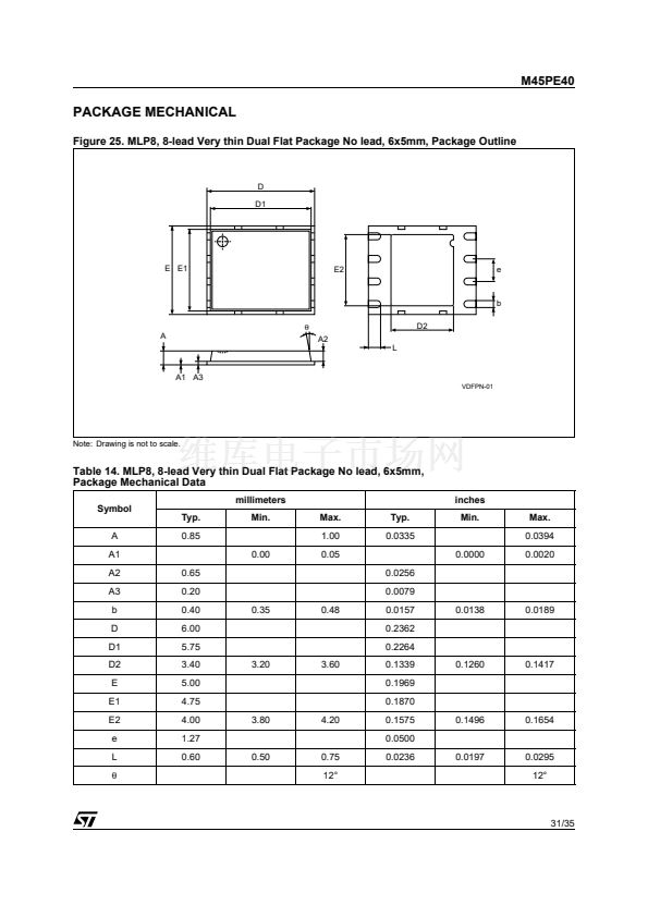
M45PE40
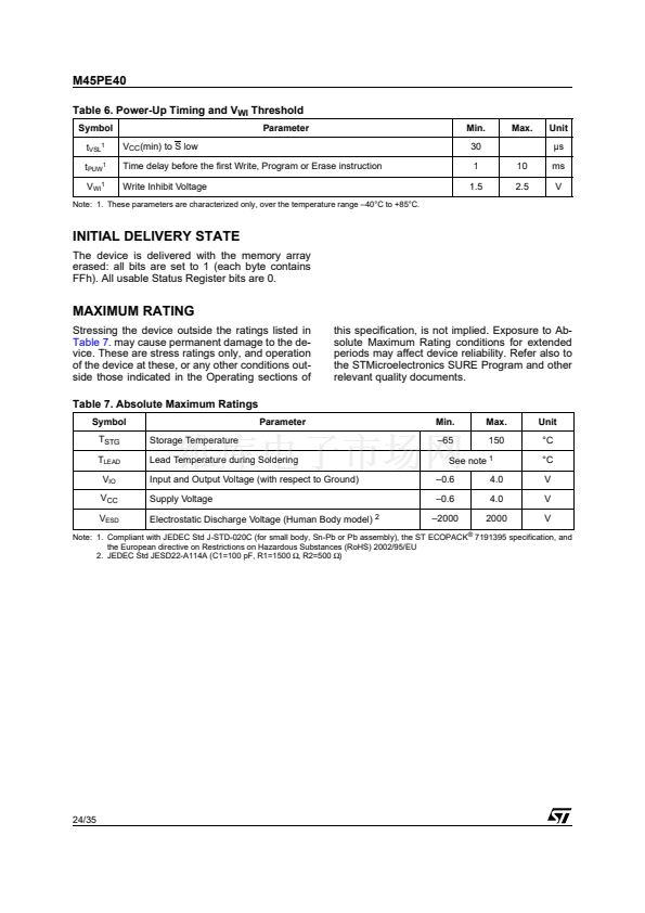
Table 12. AC Characteristics (25MHz operation)
Test conditions specified in
Table 8.
and
Table 9.
Symbol
Alt.
Parameter
Clock Frequency for the following
instructions: FAST_READ, PW, PP,
PE, SE, DP, RDP, WREN, WRDI,
RDSR
Clock Frequency for READ
instructions
t
CLH
t
CLL
Clock High Time
Clock Low Time
Clock Slew Rate
2
(peak to peak)
t
SLCH
t
CHSL
t
DVCH
t
CHDX
t
CHSH
t
SHCH
t
SHSL
t
SHQZ 2
t
CLQV
t
CLQX
t
RLRH 2
t
RHSL
t
SHRH
t
WHSL
t
SHWL
t
DP 2
t
RDP 2
t
PW (3)
t
CSH
t
DIS
t
V
t
HO
t
RST
t
REC
t
DSU
t
DH
t
CSS
S Active Setup Time (relative to C)
S Not Active Hold Time (relative to C)
Data In Setup Time
Data In Hold Time
S Active Hold Time (relative to C)
S Not Active Setup Time (relative to C)
S Deselect Time
Output Disable Time
Clock Low to Output Valid
Output Hold Time
Reset Pulse Width
Reset Recovery Time
Chip should have been deselected
before Reset is de-asserted
Write Protect Setup Time
Write Protect Hold Time
S to Deep Power-down
S High to Standby Power mode
Page Write Cycle Time (256 Bytes)
Page Write Cycle Time (n Bytes)
Page Program Cycle Time (256 Bytes)
t
PP (3)
t
PE
t
SE
Page Program Cycle Time (n Bytes)
Page Erase Cycle Time
Sector Erase Cycle Time
11
10.2+
n*0.8/256
1.2
0.4+
n*0.8/256
10
1
5
20
5
ms
ms
s
25
ms
10
50
100
3
30
0
10
3
Min.
Typ.
Max.
Unit
f
C
f
C
D.C.
25
MHz
f
R
t
CH 1
t
CL 1
D.C.
18
18
0.03
10
10
5
5
10
10
200
20
MHz
ns
ns
V/ns
ns
ns
ns
ns
ns
ns
ns
15
15
ns
ns
ns
碌s
碌s
ns
ns
ns
碌s
碌s
Note: 1. t
CH
+ t
CL
must be greater than or equal to 1/ f
C
(max)
2. Value guaranteed by characterization, not 100% tested in production.
3. When using PP and PW instructions to update consecutive Bytes, optimized timings are obtained with one sequence including all
the Bytes versus several sequences of only a few Bytes. (1


 1
1
 2
2
 3
3
 4
4
 5
5
 6
6
 7
7
 8
8
 9
9
 10
10
 11
11
 12
12
 13
13
 14
14
 15
15
 16
16
 17
17
 18
18
 19
19
 20
20
 21
21
 22
22
 23
23
 24
24
 25
25
 26
26
 27
27
 28
28
 29
29
 30
30
 31
31
 32
32
 33
33
 34
34
 35
35
