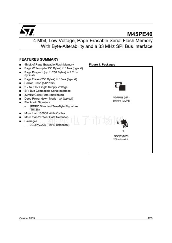
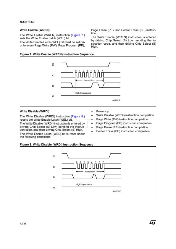
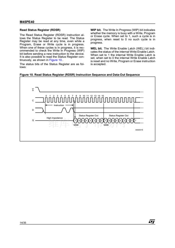
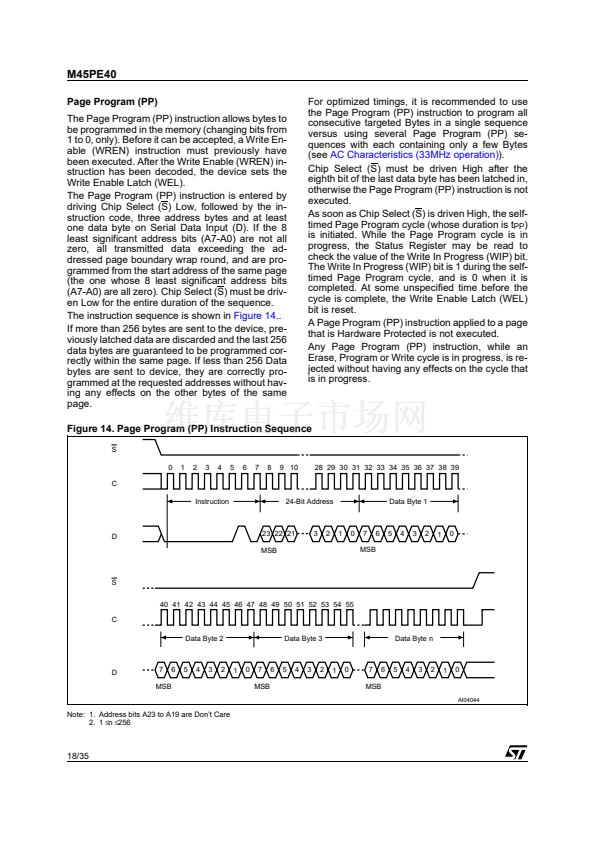
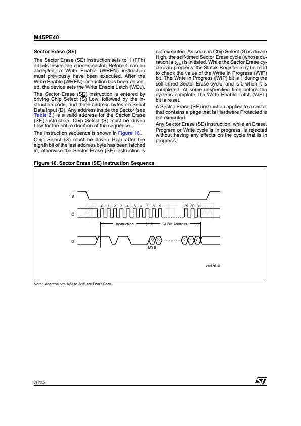
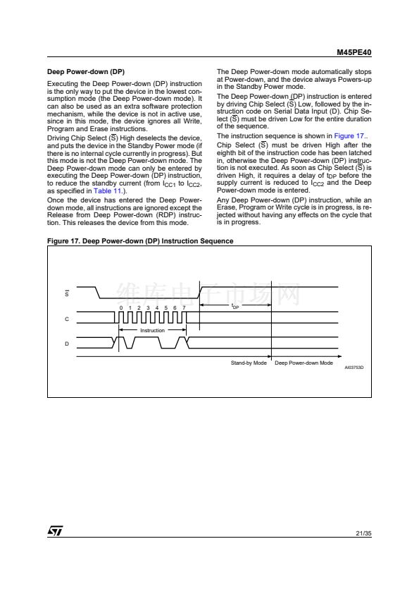
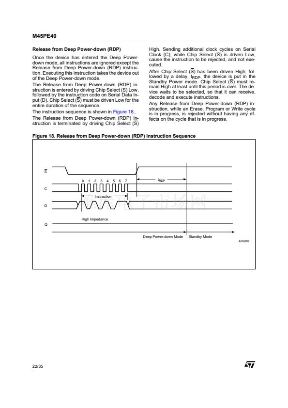
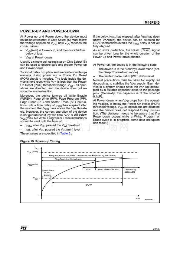
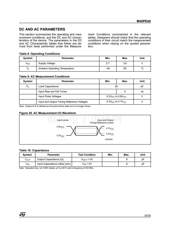
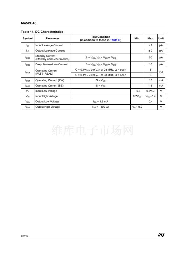
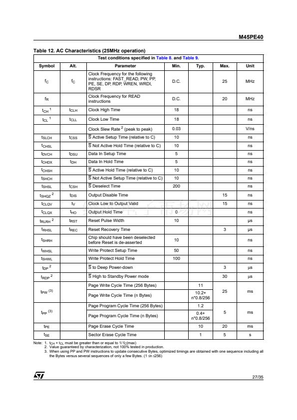
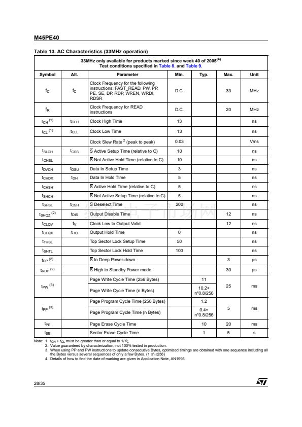
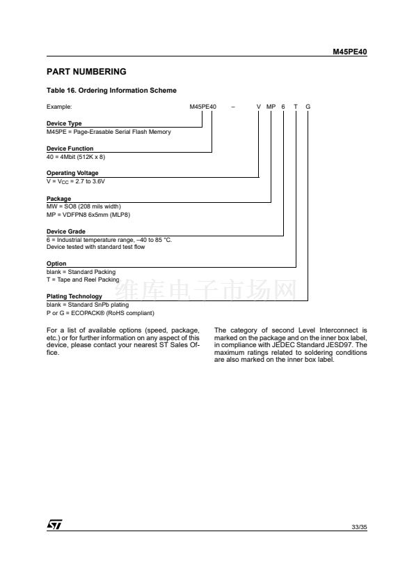
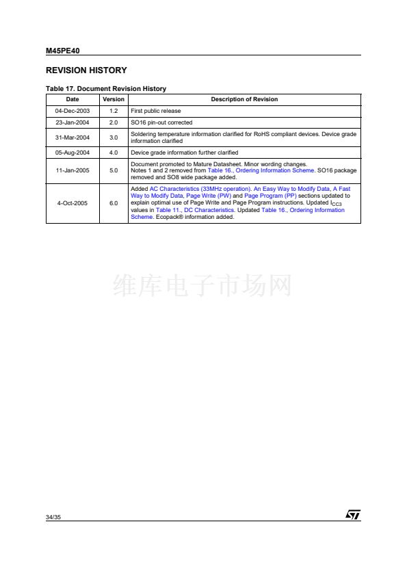
M45PE40
SUMMARY DESCRIPTION
The M45PE40 is a 4Mbit (512K x 8 bit) Serial
Paged Flash Memory accessed by a high speed
SPI-compatible bus.
The memory can be written or programmed 1 to
256 bytes at a time, using the Page Write or Page
Program instruction. The Page Write instruction
consists of an integrated Page Erase cycle fol-
lowed by a Page Program cycle.
The memory is organized as 8 sectors, each con-
taining 256 pages. Each page is 256 bytes wide.
Thus, the whole memory can be viewed as con-
sisting of 2048 pages, or 524288 bytes.
The memory can be erased a page at a time, using
the Page Erase instruction, or a sector at a time,
using the Sector Erase instruction.
In order to meet environmental requirements, ST
offers these devices in ECOPACK庐 packages.
ECOPACK庐 packages are Lead-free and RoHS
compliant.
ECOPACK is an ST trademark. ECOPACK speci-
fications are available at: www.st.com.
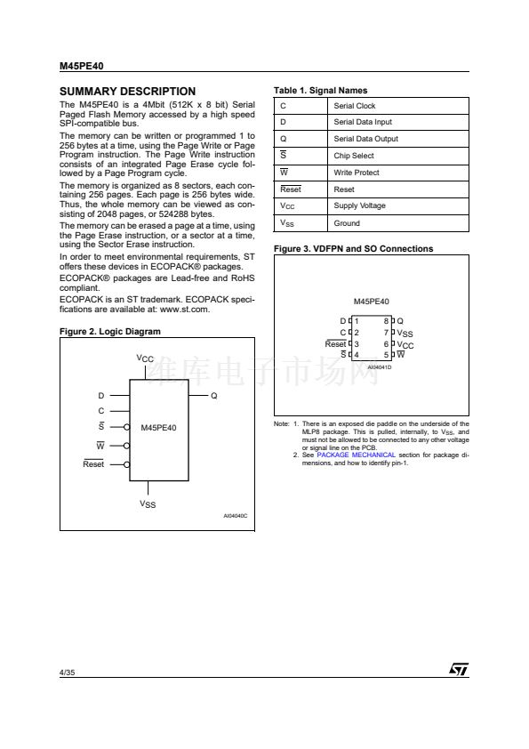
Figure 2. Logic Diagram
VCC
Table 1. Signal Names
C
D
Q
Serial Clock
Serial Data Input
Serial Data Output
Chip Select
Write Protect
Reset
Supply Voltage
Ground
S
W
Reset
V
CC
V
SS
Figure 3. VDFPN and SO Connections
M45PE40
D
C
Reset
S
1
2
3
4
8
7
6
5
AI04041D
Q
VSS
VCC
W
D
C
S
W
Reset
M45PE40
Q
Note: 1. There is an exposed die paddle on the underside of the
MLP8 package. This is pulled, internally, to V
SS
, and
must not be allowed to be connected to any other voltage
or signal line on the PCB.
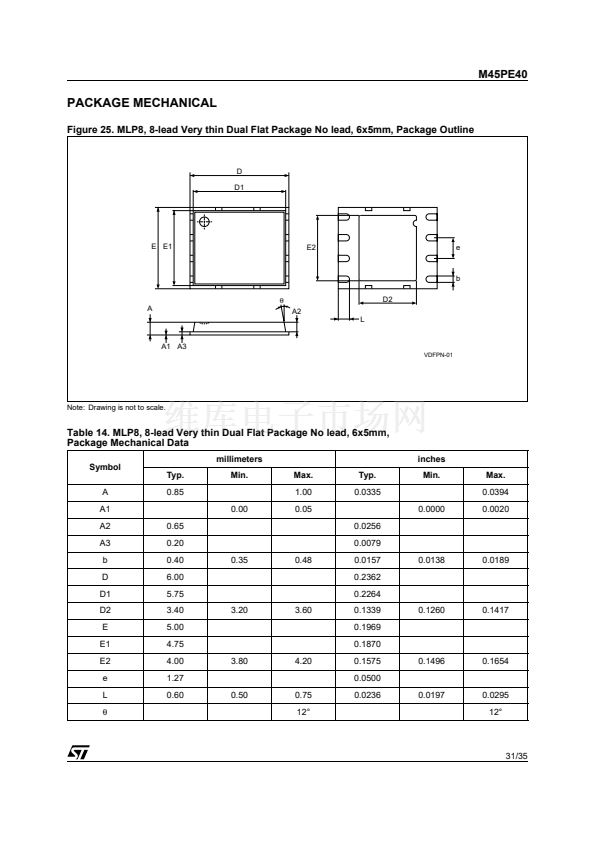
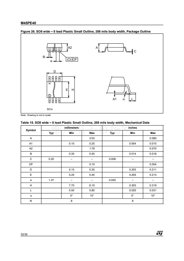
2. See
PACKAGE MECHANICAL
section for package di-
mensions, and how to identify pin-1.
VSS
AI04040C
4/35


 1
1
 2
2
 3
3
 4
4
 5
5
 6
6
 7
7
 8
8
 9
9
 10
10
 11
11
 12
12
 13
13
 14
14
 15
15
 16
16
 17
17
 18
18
 19
19
 20
20
 21
21
 22
22
 23
23
 24
24
 25
25
 26
26
 27
27
 28
28
 29
29
 30
30
 31
31
 32
32
 33
33
 34
34
 35
35
