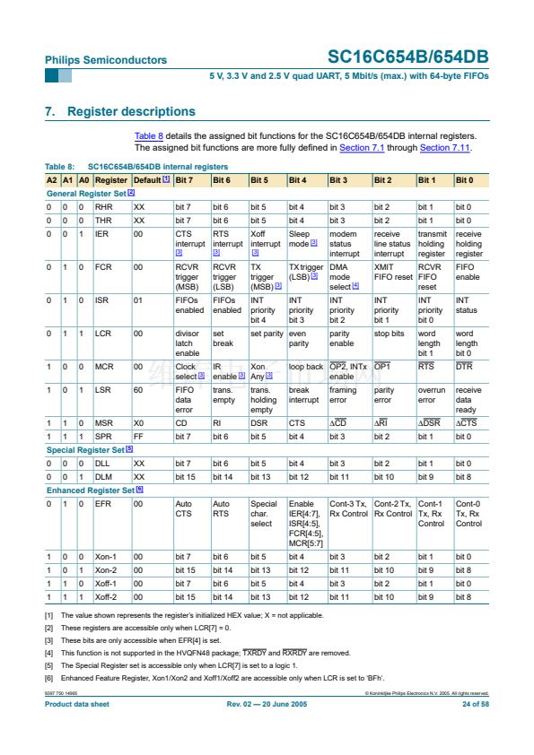
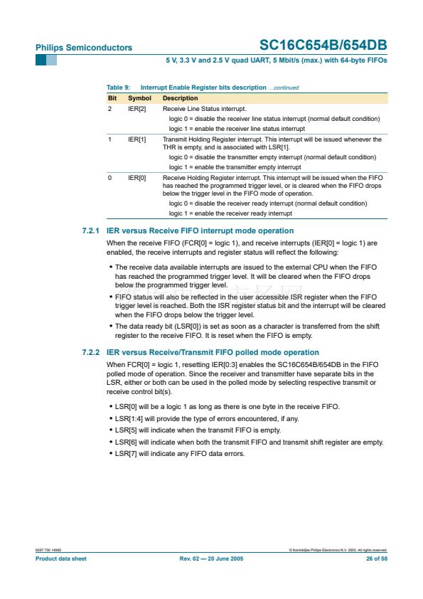
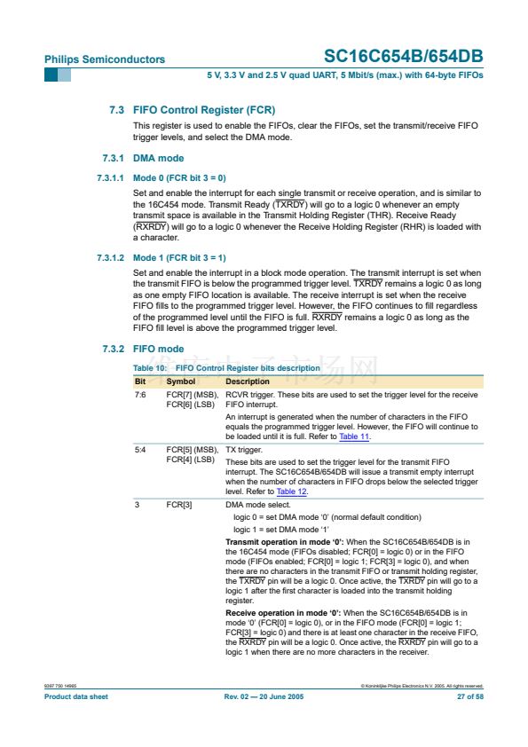
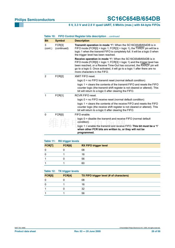
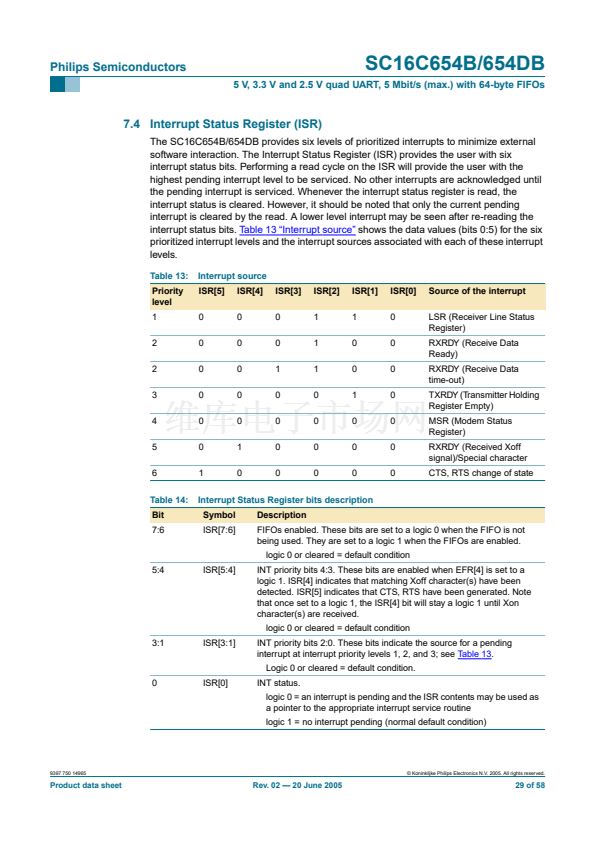
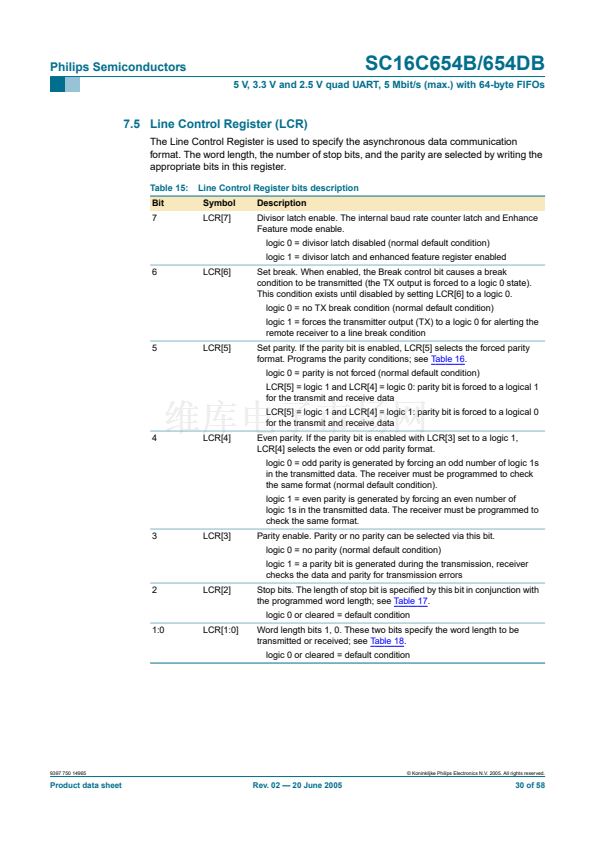
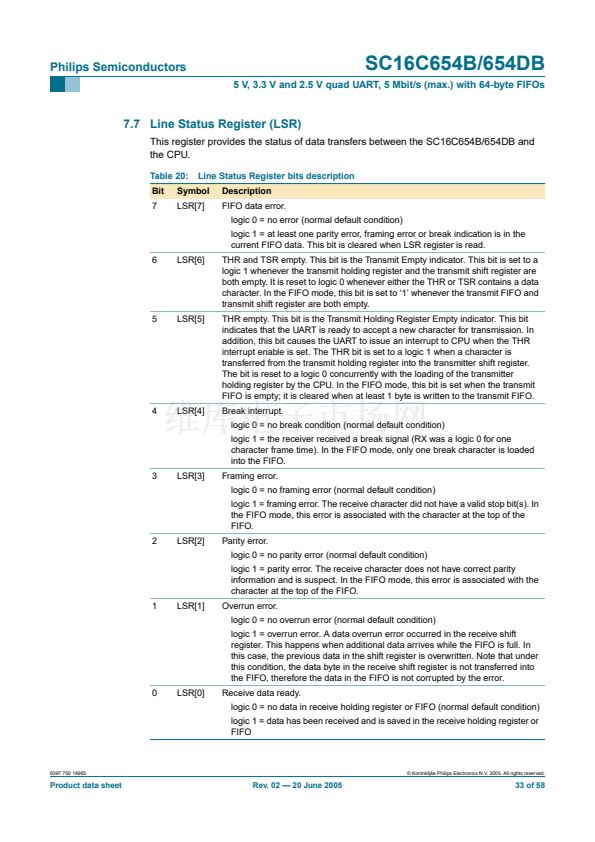
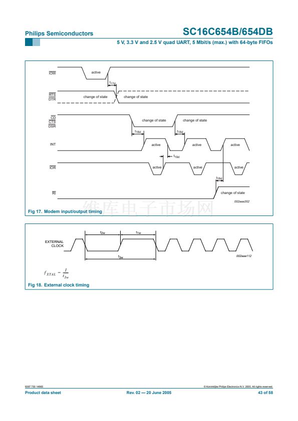
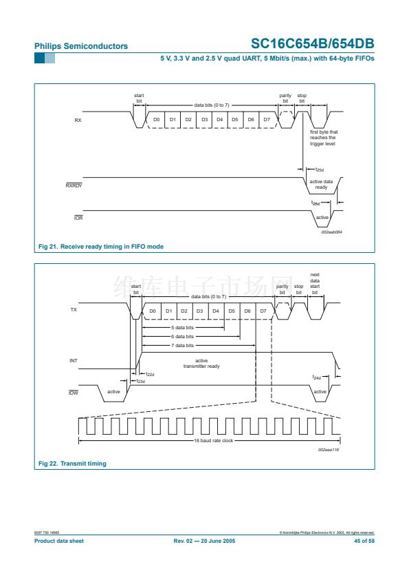
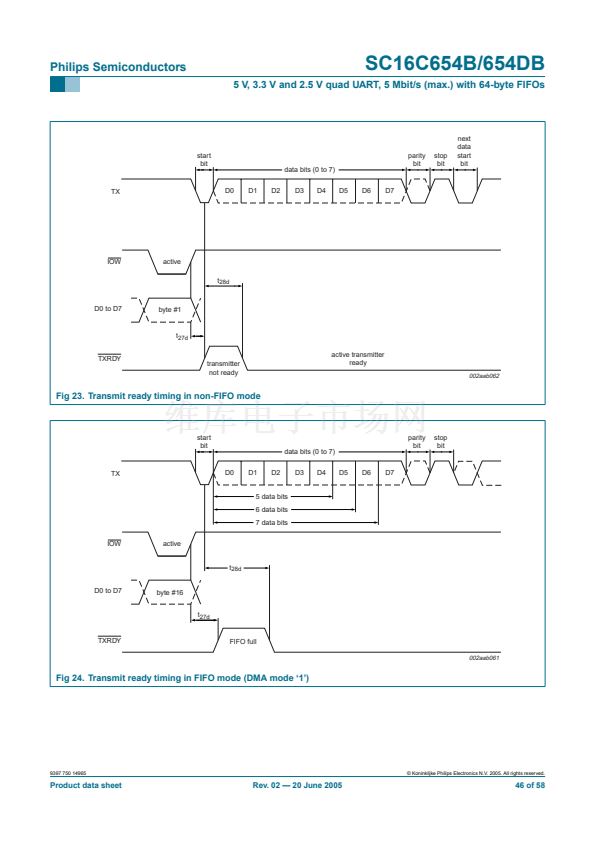
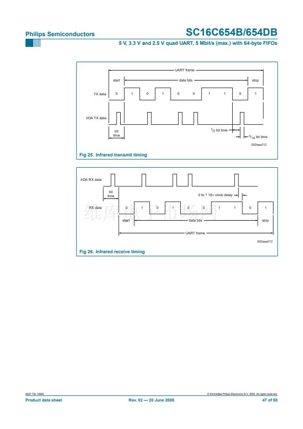
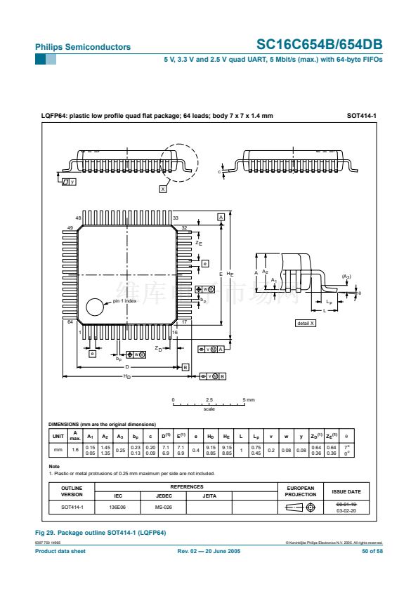
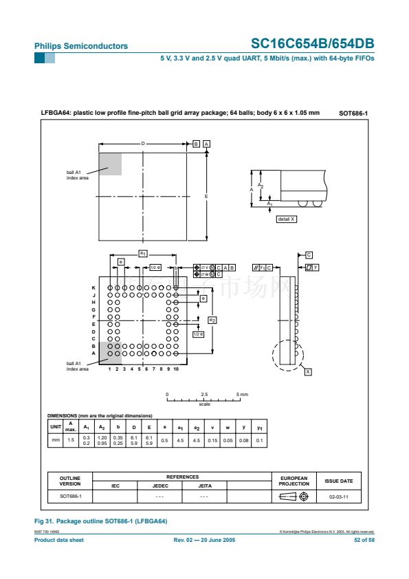
鈦?/div>
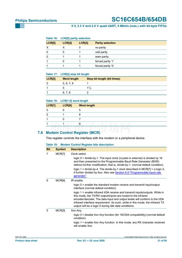
2
2
LCR[1:0] word length
LCR[0]
0
1
0
1
Word length
5
6
7
8
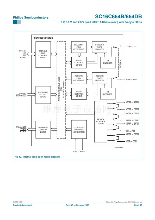
7.6 Modem Control Register (MCR)
This register controls the interface with the modem or a peripheral device.
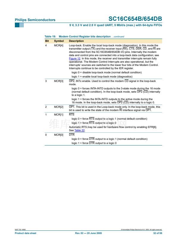
Table 19:
Bit
7
Modem Control Register bits description
Description
Clock select.
logic 0 = divide-by-1. The input clock (crystal or external) is divided by 16
and then presented to the Programmable Baud Rate Generator (BGR)
without further modi铿乧ation, that is, divide-by-1. (normal default condition).
logic 1 = divide-by-4. The divide-by-1 clock described in MCR[7] = a logic 0,
if further divided by four. Also see
Section 6.9 鈥淧rogrammable baud rate
generator鈥?
6
MCR[6]
IR enable.
logic 0 = enable the standard modem receive and transmit input/output
interface (normal default condition)
logic 1 = enable infrared IrDA receive and transmit inputs/outputs. While in
this mode, the TX/RX output/inputs are routed to the infrared
encoder/decoder. The data input and output levels will conform to the IrDA
infrared interface requirement. As such, while in this mode, the infrared TX
output will be a logic 0 during idle data conditions.
5
MCR[5]
Xon Any.
logic 0 = disable Xon Any function (for 16C554 compatibility) (normal default
condition)
logic 1 = enable Xon Any function. In this mode, any RX character received
will enable Xon
Symbol
MCR[7]
9397 750 14965
漏 Koninklijke Philips Electronics N.V. 2005. All rights reserved.
Product data sheet
Rev. 02 鈥?20 June 2005
31 of 58


 1
1
 2
2
 3
3
 4
4
 5
5
 6
6
 7
7
 8
8
 9
9
 10
10
 11
11
 12
12
 13
13
 14
14
 15
15
 16
16
 17
17
 18
18
 19
19
 20
20
 21
21
 22
22
 23
23
 24
24
 25
25
 26
26
 27
27
 28
28
 29
29
 30
30
 31
31
 32
32
 33
33
 34
34
 35
35
 36
36
 37
37
 38
38
 39
39
 40
40
 41
41
 42
42
 43
43
 44
44
 45
45
 46
46
 47
47
 48
48
 49
49
 50
50
 51
51
 52
52
 53
53
 54
54
 55
55
 56
56
 57
57
 58
58
