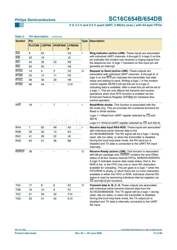
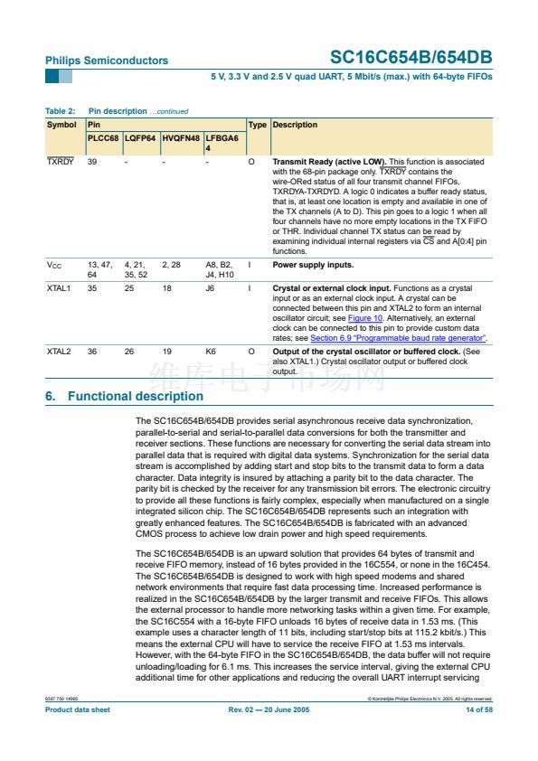
Philips Semiconductors
SC16C654B/654DB
5 V, 3.3 V and 2.5 V quad UART, 5 Mbit/s (max.) with 64-byte FIFOs
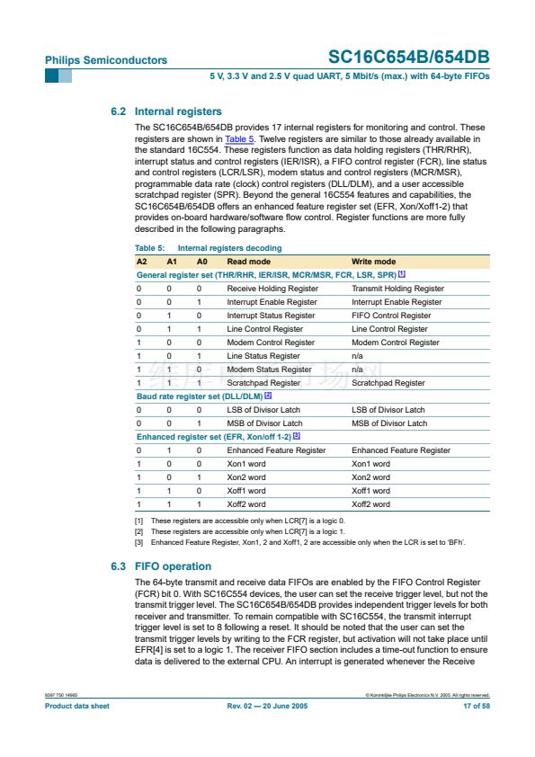
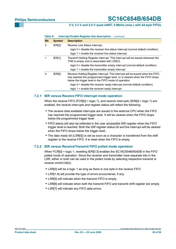
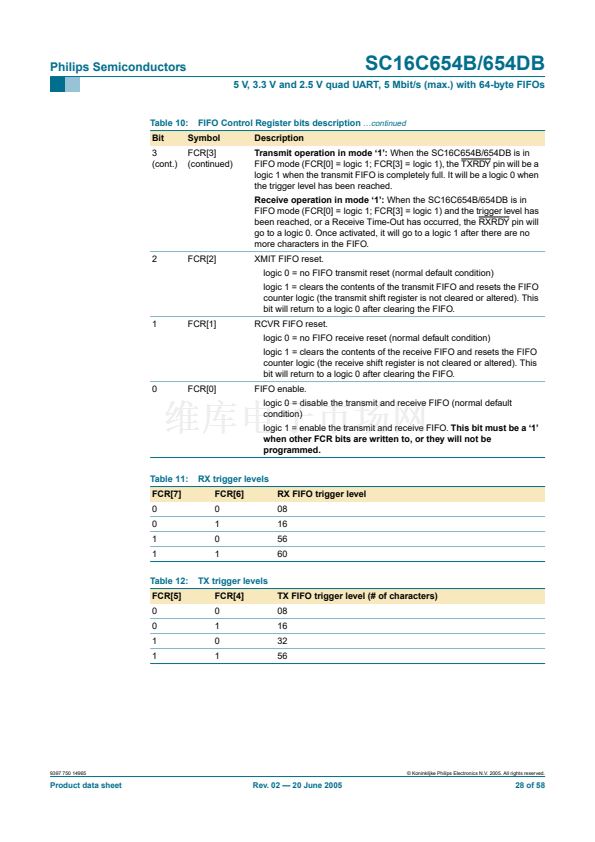
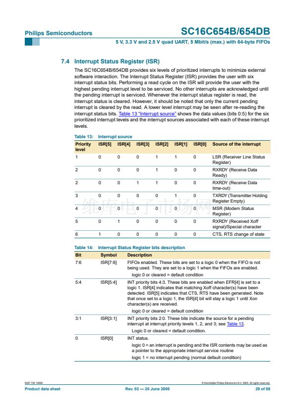
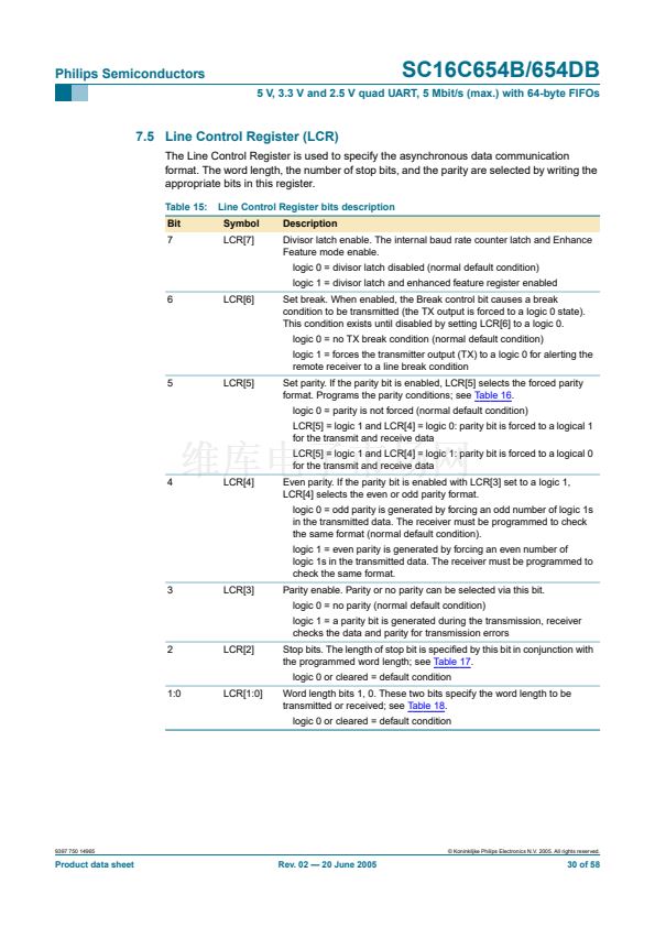
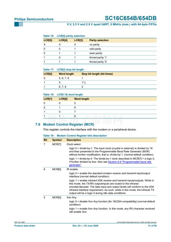
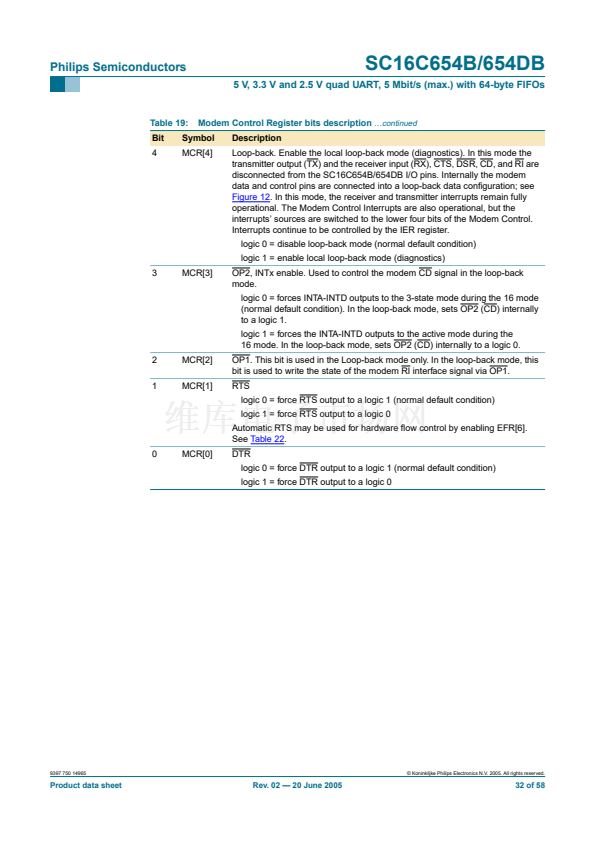
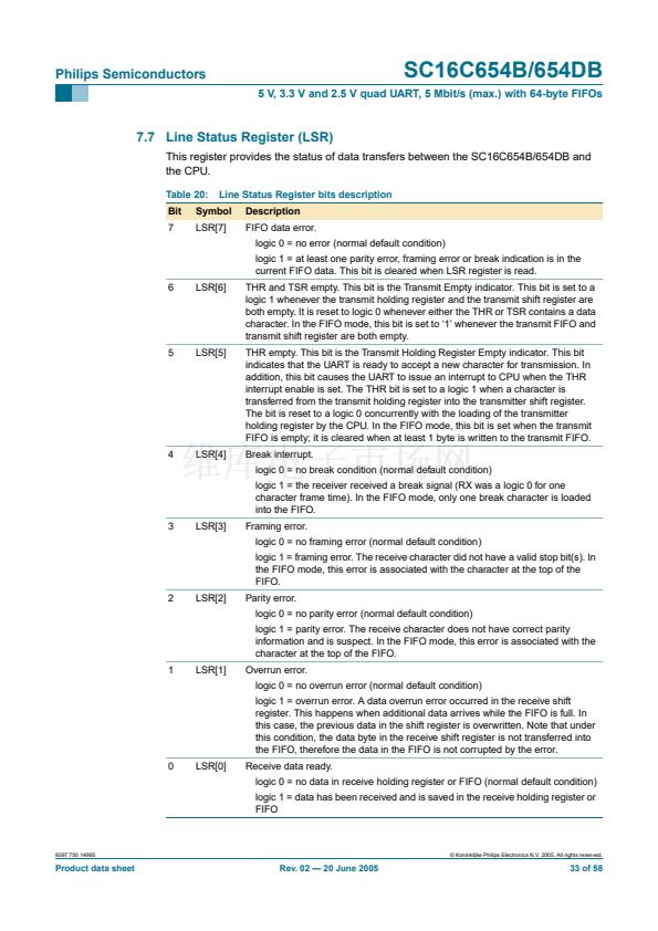
7.7 Line Status Register (LSR)
This register provides the status of data transfers between the SC16C654B/654DB and
the CPU.
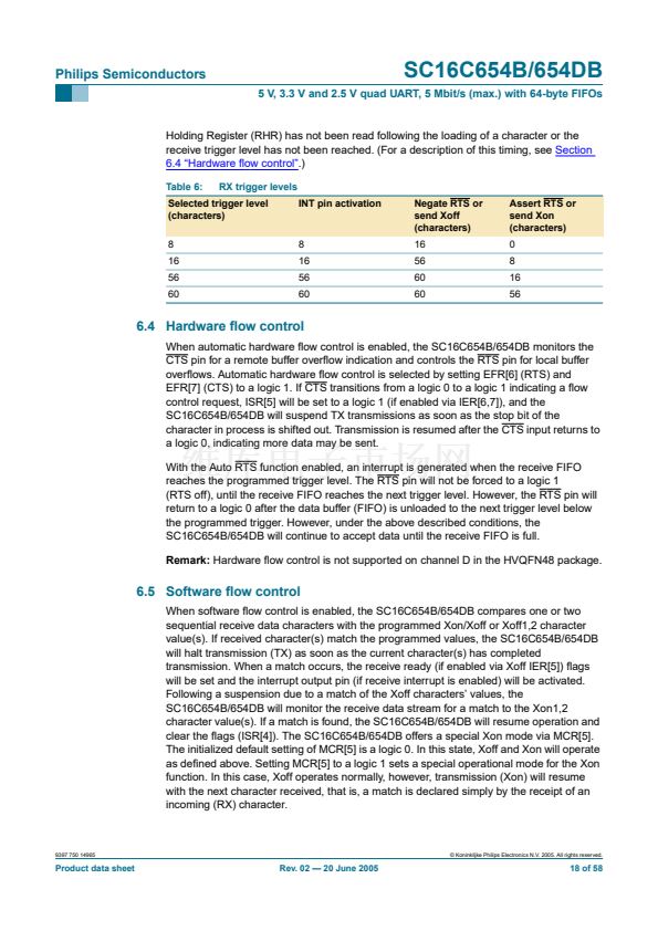
Table 20:
Bit
7
Line Status Register bits description
Description
FIFO data error.
logic 0 = no error (normal default condition)
logic 1 = at least one parity error, framing error or break indication is in the
current FIFO data. This bit is cleared when LSR register is read.
6
LSR[6]
THR and TSR empty. This bit is the Transmit Empty indicator. This bit is set to a
logic 1 whenever the transmit holding register and the transmit shift register are
both empty. It is reset to logic 0 whenever either the THR or TSR contains a data
character. In the FIFO mode, this bit is set to 鈥?鈥?whenever the transmit FIFO and
transmit shift register are both empty.
THR empty. This bit is the Transmit Holding Register Empty indicator. This bit
indicates that the UART is ready to accept a new character for transmission. In
addition, this bit causes the UART to issue an interrupt to CPU when the THR
interrupt enable is set. The THR bit is set to a logic 1 when a character is
transferred from the transmit holding register into the transmitter shift register.
The bit is reset to a logic 0 concurrently with the loading of the transmitter
holding register by the CPU. In the FIFO mode, this bit is set when the transmit
FIFO is empty; it is cleared when at least 1 byte is written to the transmit FIFO.
Break interrupt.
logic 0 = no break condition (normal default condition)
logic 1 = the receiver received a break signal (RX was a logic 0 for one
character frame time). In the FIFO mode, only one break character is loaded
into the FIFO.
3
LSR[3]
Framing error.
logic 0 = no framing error (normal default condition)
logic 1 = framing error. The receive character did not have a valid stop bit(s). In
the FIFO mode, this error is associated with the character at the top of the
FIFO.
2
LSR[2]
Parity error.
logic 0 = no parity error (normal default condition)
logic 1 = parity error. The receive character does not have correct parity
information and is suspect. In the FIFO mode, this error is associated with the
character at the top of the FIFO.
1
LSR[1]
Overrun error.
logic 0 = no overrun error (normal default condition)
logic 1 = overrun error. A data overrun error occurred in the receive shift
register. This happens when additional data arrives while the FIFO is full. In
this case, the previous data in the shift register is overwritten. Note that under
this condition, the data byte in the receive shift register is not transferred into
the FIFO, therefore the data in the FIFO is not corrupted by the error.
0
LSR[0]
Receive data ready.
logic 0 = no data in receive holding register or FIFO (normal default condition)
logic 1 = data has been received and is saved in the receive holding register or
FIFO
Symbol
LSR[7]
5
LSR[5]
4
LSR[4]
9397 750 14965
漏 Koninklijke Philips Electronics N.V. 2005. All rights reserved.
Product data sheet
Rev. 02 鈥?20 June 2005
33 of 58


 1
1
 2
2
 3
3
 4
4
 5
5
 6
6
 7
7
 8
8
 9
9
 10
10
 11
11
 12
12
 13
13
 14
14
 15
15
 16
16
 17
17
 18
18
 19
19
 20
20
 21
21
 22
22
 23
23
 24
24
 25
25
 26
26
 27
27
 28
28
 29
29
 30
30
 31
31
 32
32
 33
33
 34
34
 35
35
 36
36
 37
37
 38
38
 39
39
 40
40
 41
41
 42
42
 43
43
 44
44
 45
45
 46
46
 47
47
 48
48
 49
49
 50
50
 51
51
 52
52
 53
53
 54
54
 55
55
 56
56
 57
57
 58
58
