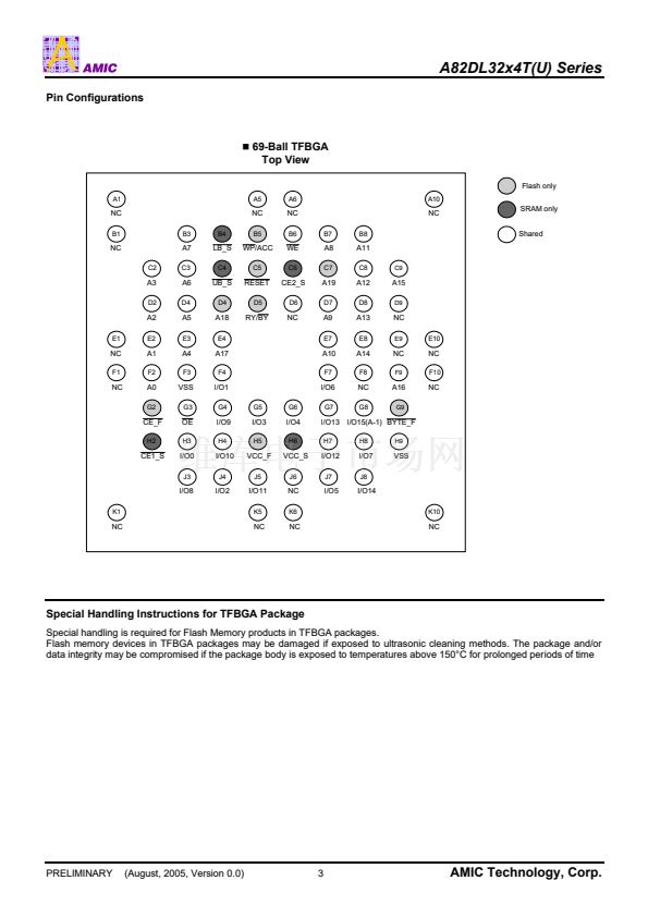
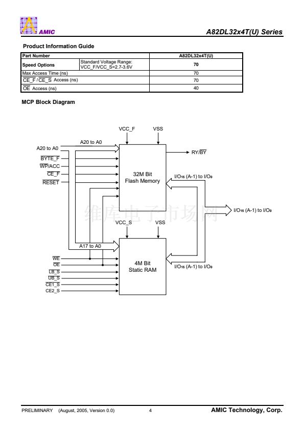
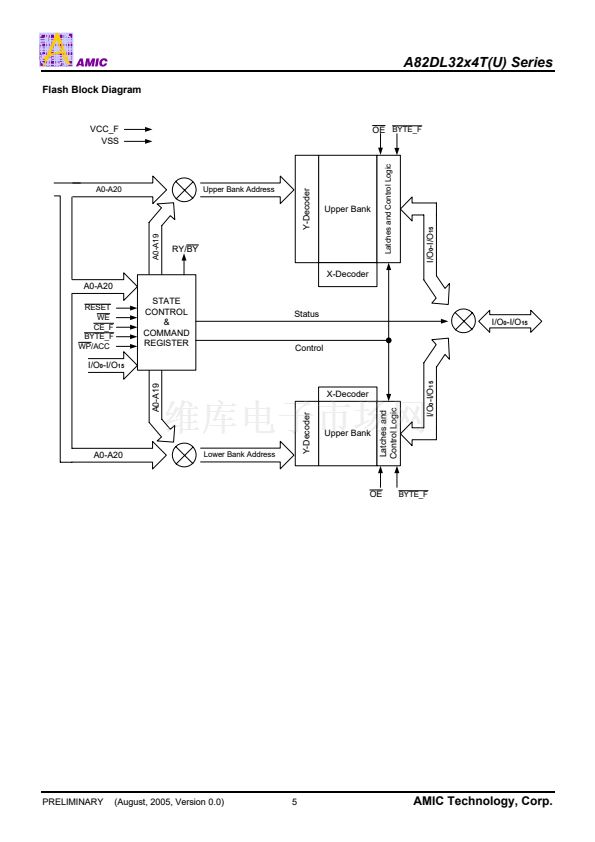
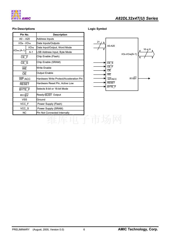
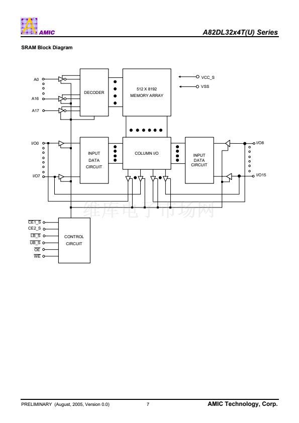
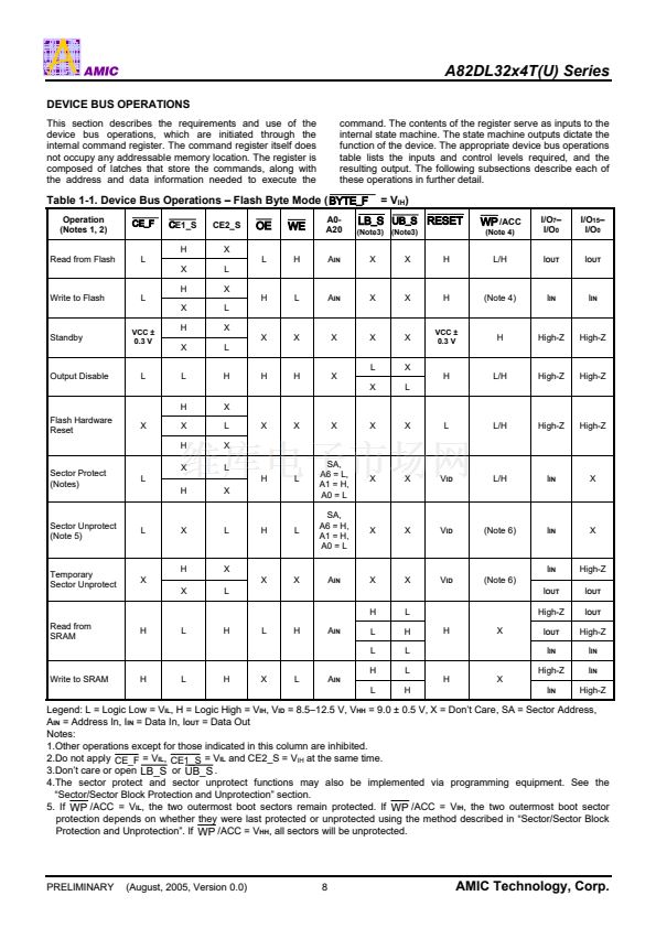
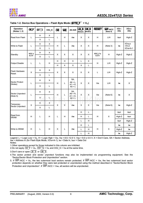
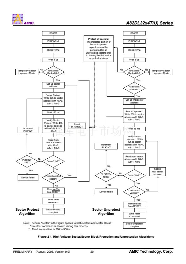
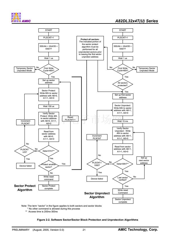
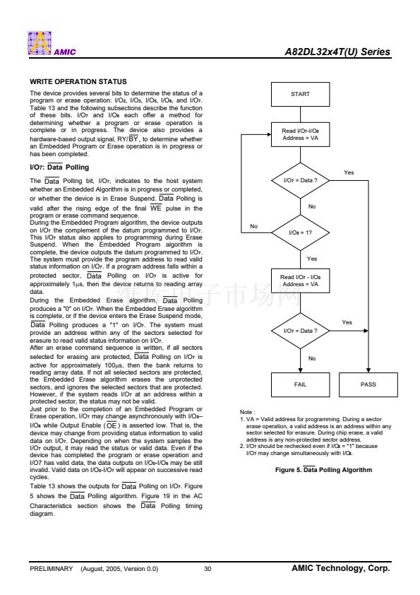
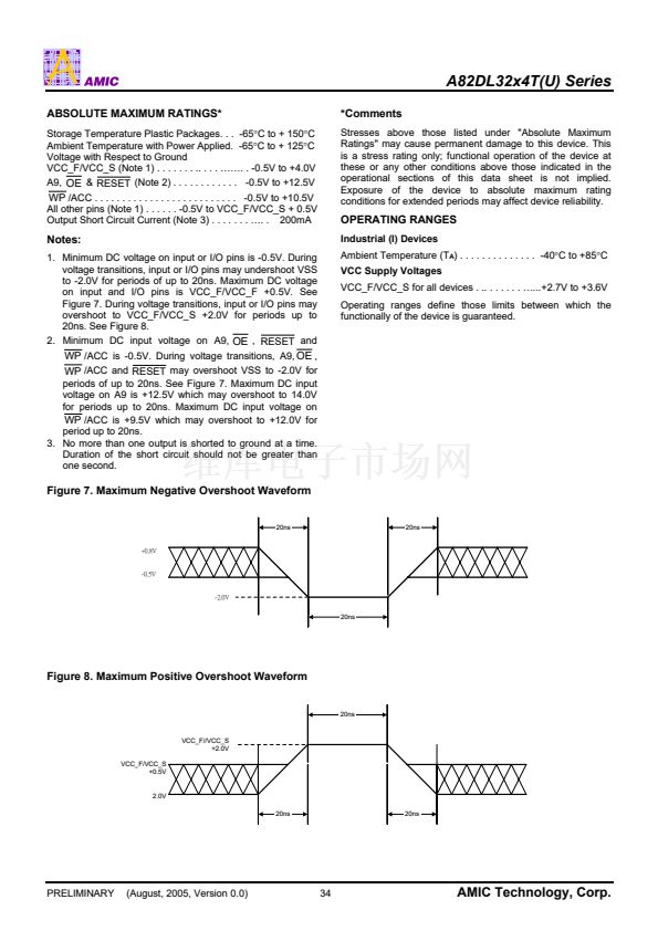
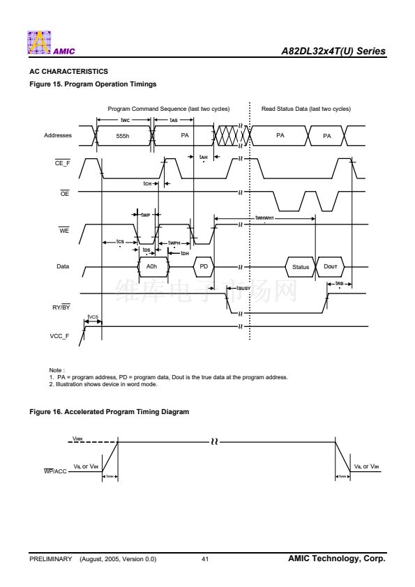
A82DL32x4T(U) Series
Automatic Sleep Mode
The automatic sleep mode minimizes Flash device energy
consumption. The device automatically enables this mode
when addresses remain stable for t
ACC
+30ns. The automatic
sleep mode is independent of the
CE_F
,
WE
and
OE
control signals. Standard address access timings provide
new data when addresses are changed. While in sleep
mode, output data is latched and always available to the
system. I
CC4_F
in the DC Characteristics table represents the
automatic sleep mode current specification.
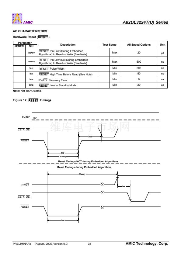
The
RESET
pin may be tied to the system reset circuitry. A
system reset would thus also reset the Flash memory,
enabling the system to read the boot-up firmware from the
Flash memory.
If
RESET
is asserted during a program or erase operation,
the RY/
BY
pin remains a 鈥?鈥?(busy) until the internal reset
operation is complete, which requires a time t
READY
(during
Embedded Algorithms). The system can thus monitor
RY/
BY
to determine whether the reset operation is
complete. If
RESET
is asserted when a program or erase
operation is not executing (RY/
BY
pin is 鈥?鈥?, the reset
operation is completed within a time of t
READY
(not during
Embedded Algorithms). The system can read data t
RH
after
the
RESET
pin return to V
IH
.
Refer to the AC Characteristics tables for
RESET
parameters and diagram.
RESET
: Hardware Reset Pin
The
RESET
pin provides a hardware method of resetting
the device to reading array data. When the system drives the
RESET
pin low for at least a period of t
RP
, the device
immediately terminates any operation in progress, tristates
all data output pins, and ignores all read/write attempts for
the duration of the
RESET
pulse. The device also resets the
internal state machine to reading array data. The operation
that was interrupted should be reinitiated once the device is
ready to accept another command sequence, to ensure data
integrity.
Current is reduced for the duration of the
RESET
pulse.
When
RESET
is held at VSS
卤
0.3V, the device draws
CMOS standby current (I
CC4_F
). If
RESET
is held at V
IL
but
not within VSS
卤
0.3V, the standby current will be greater.
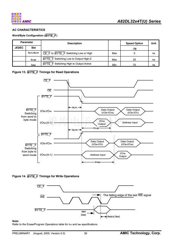
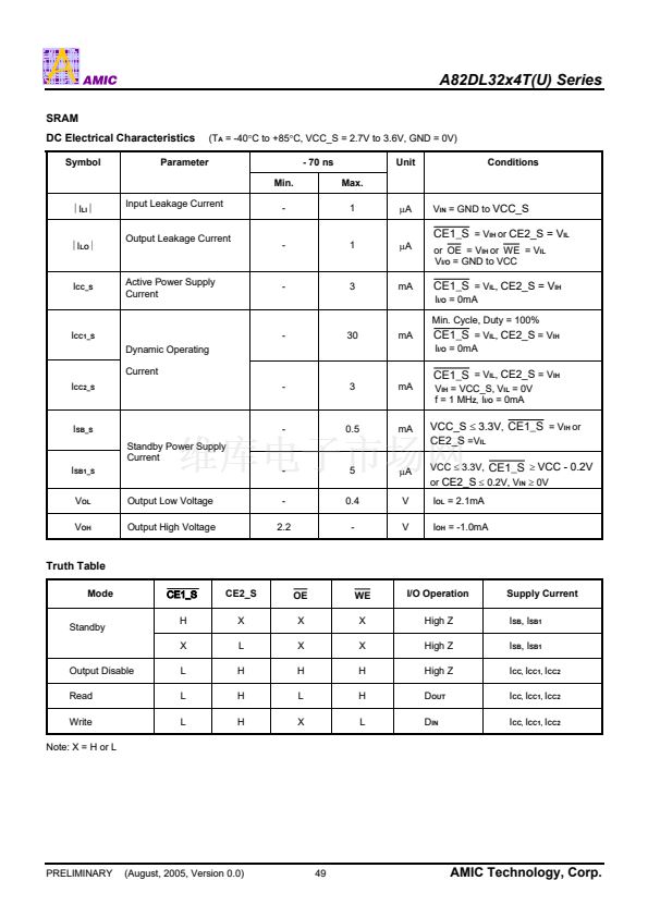
Output Disable Mode
When the
OE
input is at V
IH
, output from the device is
disabled. The output pins are placed in the high impedance
state.
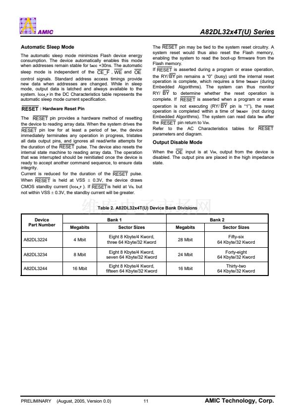
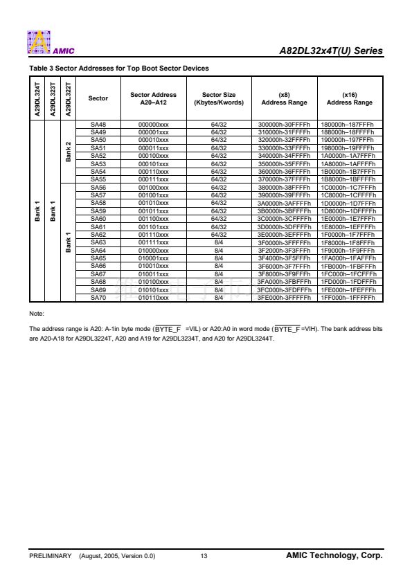
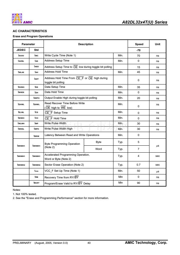
Table 2. A82DL32x4T(U) Device Bank Divisions
Device
Part Number
A82DL3224
A82DL3234
A82DL3244
Bank 1
Megabits
4 Mbit
8 Mbit
16 Mbit
Sector Sizes
Eight 8 Kbyte/4 Kword,
three 64 Kbyte/32 Kword
Eight 8 Kbyte/4 Kword,
seven 64 Kbyte/32 Kword
Eight 8 Kbyte/4 Kword,
fifteen 64 Kbyte/32 Kword
Megabits
28 Mbit
24 Mbit
16 Mbit
Bank 2
Sector Sizes
Fifty-six
64 Kbyte/32 Kword
Forty-eight
64 Kbyte/32 Kword
Thirty-two
64 Kbyte/32 Kword
PRELIMINARY
(August, 2005, Version 0.0)
11
AMIC Technology, Corp.


 1
1
 2
2
 3
3
 4
4
 5
5
 6
6
 7
7
 8
8
 9
9
 10
10
 11
11
 12
12
 13
13
 14
14
 15
15
 16
16
 17
17
 18
18
 19
19
 20
20
 21
21
 22
22
 23
23
 24
24
 25
25
 26
26
 27
27
 28
28
 29
29
 30
30
 31
31
 32
32
 33
33
 34
34
 35
35
 36
36
 37
37
 38
38
 39
39
 40
40
 41
41
 42
42
 43
43
 44
44
 45
45
 46
46
 47
47
 48
48
 49
49
 50
50
 51
51
 52
52
 53
53
 54
54
 55
55
 56
56
 57
57
 58
58
 59
59
 60
60
