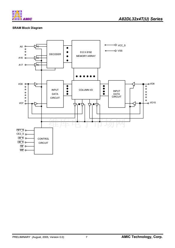
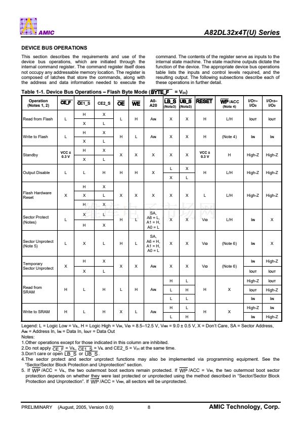
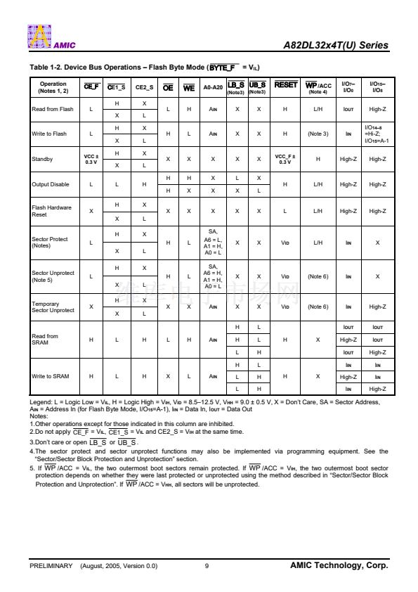
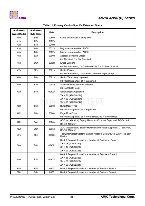
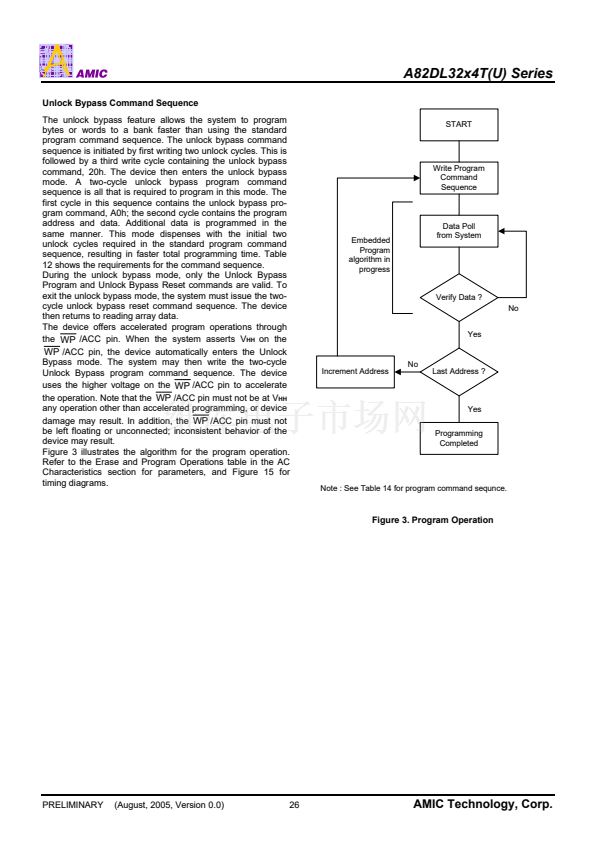
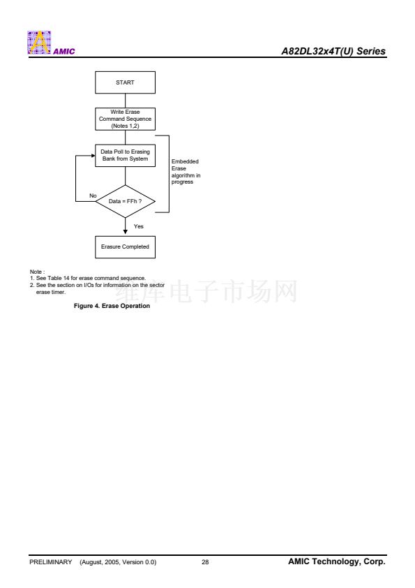
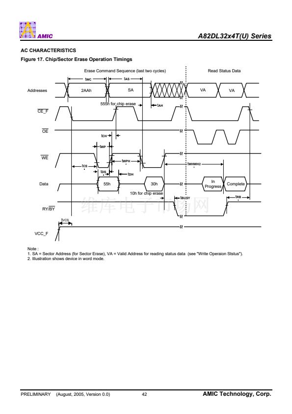
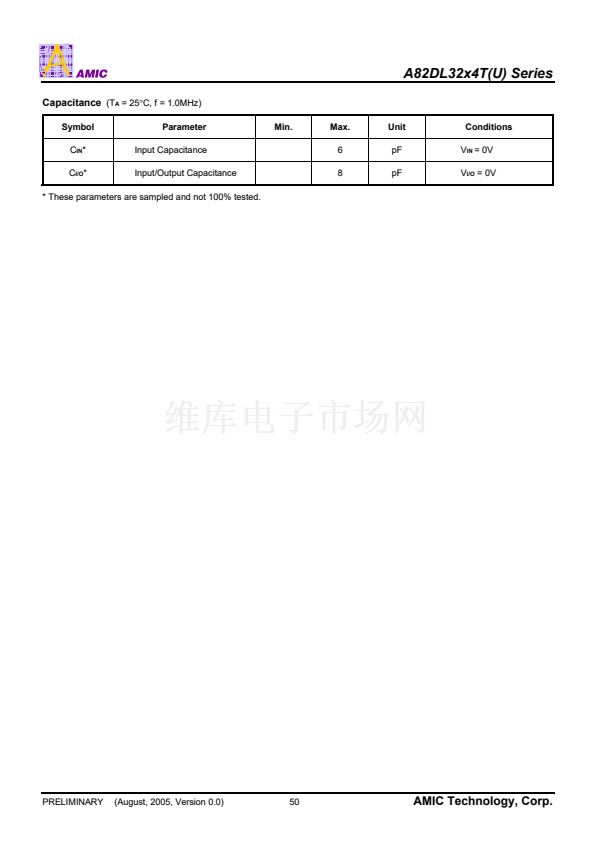
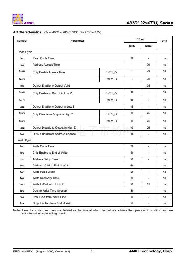
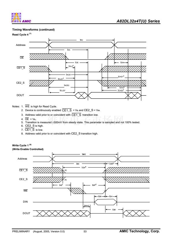
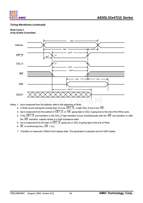
A82DL32x4T(U) Series
WRITE OPERATION STATUS
The device provides several bits to determine the status of a
program or erase operation: I/O
2
, I/O
3
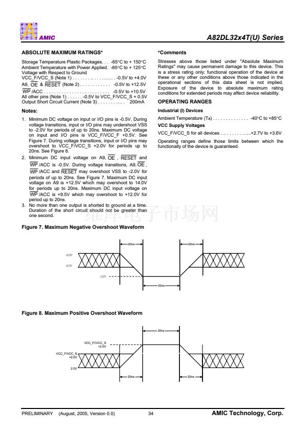
, I/O
5
, I/O
6
, and I/O
7
.
Table 13 and the following subsections describe the function
of these bits. I/O
7
and I/O
6
each offer a method for
determining whether a program or erase operation is
complete or in progress. The device also provides a
hardware-based output signal, RY/
BY
, to determine whether
an Embedded Program or Erase operation is in progress or
has been completed.
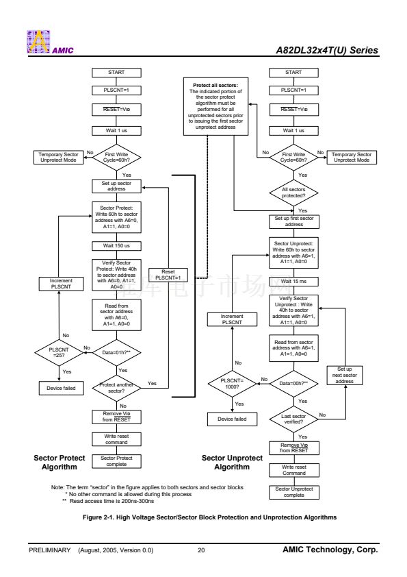
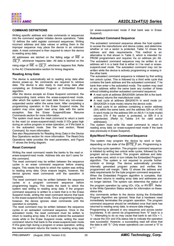
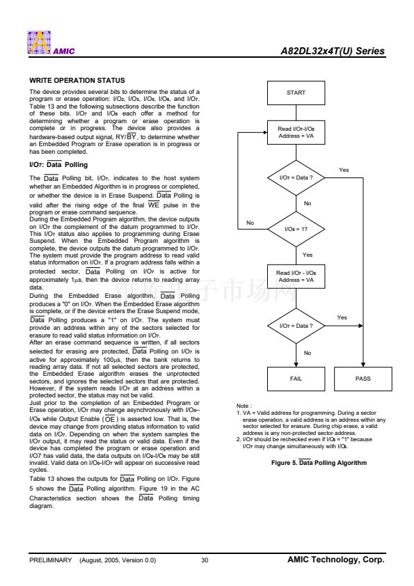
START
Read I/O
7
-I/O
0
Address = VA
I/O
7
:
Data
Polling
The
Data
Polling bit, I/O
7
, indicates to the host system
whether an Embedded Algorithm is in progress or completed,
or whether the device is in Erase Suspend.
Data
Polling is
valid after the rising edge of the final
WE
pulse in the
program or erase command sequence.
During the Embedded Program algorithm, the device outputs
on I/O
7
the complement of the datum programmed to I/O
7
.
This I/O
7
status also applies to programming during Erase
Suspend. When the Embedded Program algorithm is
complete, the device outputs the datum programmed to I/O
7
.
The system must provide the program address to read valid
status information on I/O
7
. If a program address falls within a
protected sector,
Data
Polling on I/O
7
is active for
approximately 1碌s, then the device returns to reading array
data.
During the Embedded Erase algorithm,
Data
Polling
produces a "0" on I/O
7
. When the Embedded Erase algorithm
is complete, or if the device enters the Erase Suspend mode,
Data
Polling produces a "1" on I/O
7
. The system must
provide an address within any of the sectors selected for
erasure to read valid status information on I/O
7
.
After an erase command sequence is written, if all sectors
selected for erasing are protected,
Data
Polling on I/O
7
is
active for approximately 100碌s, then the bank returns to
reading array data. If not all selected sectors are protected,
the Embedded Erase algorithm erases the unprotected
sectors, and ignores the selected sectors that are protected.
However, if the system reads I/O
7
at an address within a
protected sector, the status may not be valid.
Just prior to the completion of an Embedded Program or
Erase operation, I/O
7
may change asynchronously with I/O
0
鈥?/div>
I/O
6
while Output Enable (
OE
) is asserted low. That is, the
device may change from providing status information to valid
data on I/O
7
. Depending on when the system samples the
I/O
7
output, it may read the status or valid data. Even if the
device has completed the program or erase operation and
I/O7 has valid data, the data outputs on I/O
0
-I/O
6
may be still
invalid. Valid data on I/O
0
-I/O
7
will appear on successive read
cycles.
Table 13 shows the outputs for
Data
Polling on I/O
7
. Figure
5 shows the
Data
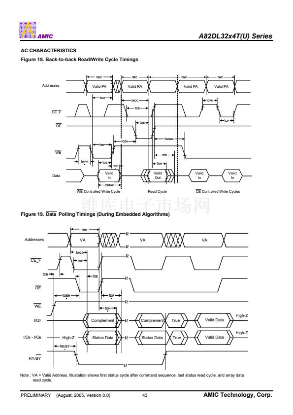
Polling algorithm. Figure 19 in the AC
Characteristics section shows the
Data
Polling timing
diagram.
I/O
7
= Data ?
Yes
No
No
I/O
5
= 1?
Yes
Read I/O
7
- I/O
0
Address = VA
Yes
I/O
7
= Data ?
No
FAIL
PASS
Note :
1. VA = Valid address for programming. During a sector
erase operation, a valid address is an address within any
sector selected for erasure. During chip erase, a valid
address is any non-protected sector address.
2. I/O
7
should be rechecked even if I/O
5
= "1" because
I/O
7
may change simultaneously with I/O .
5
Figure 5. Data Polling Algorithm
PRELIMINARY
(August, 2005, Version 0.0)
30
AMIC Technology, Corp.


 1
1
 2
2
 3
3
 4
4
 5
5
 6
6
 7
7
 8
8
 9
9
 10
10
 11
11
 12
12
 13
13
 14
14
 15
15
 16
16
 17
17
 18
18
 19
19
 20
20
 21
21
 22
22
 23
23
 24
24
 25
25
 26
26
 27
27
 28
28
 29
29
 30
30
 31
31
 32
32
 33
33
 34
34
 35
35
 36
36
 37
37
 38
38
 39
39
 40
40
 41
41
 42
42
 43
43
 44
44
 45
45
 46
46
 47
47
 48
48
 49
49
 50
50
 51
51
 52
52
 53
53
 54
54
 55
55
 56
56
 57
57
 58
58
 59
59
 60
60
