A82DL32x4T(U) Series
Stacked Multi-Chip Package (MCP) Flash Memory and SRAM,
A82DL32x4T(U) 32 Megabit (4Mx8 Bit/2Mx16 Bit) CMOS 3.3 Volt-only,
Simultaneous Operation Flash Memory and 4M (256Kx16 Bit) Static RAM
Preliminary
DISTINCTIVE CHARACTERISTICS
MCP Features
Single power supply operation 2.7 to 3.6 volt
High Performance
- Access time as fast as 70ns
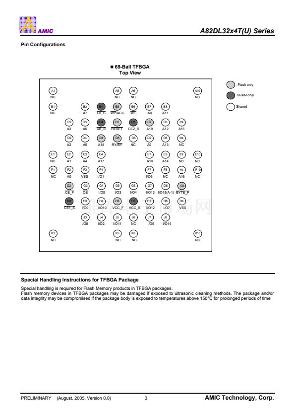
Package 69-Ball TFBGA (8x11x1.4 mm)
Industrial operating temperature range: -40掳C to 85掳C
for 鈥揢; -25掳C to 85掳C for 鈥揑
-
Suspends erase operations to allow programming in
same bank
Data
Polling and Toggle Bit
-
Provides a software method of detecting the status of
program or erase cycles
Unlock Bypass Program command
-
Reduces overall programming time when issuing
multiple program command sequences
HARDWARE FEATURES
Any combination of sectors can be erased
Ready/
Busy
output (RY/
BY
)
- Hardware method for detecting program or erase cycle
completion
Hardware reset pin (
RESET
)
- Hardware method of resetting the internal state machine
to reading array data
WP
/ACC input pin
- Write protect (
WP
) function allows protection of two
outermost boot sectors, regardless of sector protect
status
- Acceleration (ACC) function accelerates program timing
Sector protection
- Hardware method of locking a sector, either in-system or
using programming equipment, to prevent any program
or erase operation within that sector
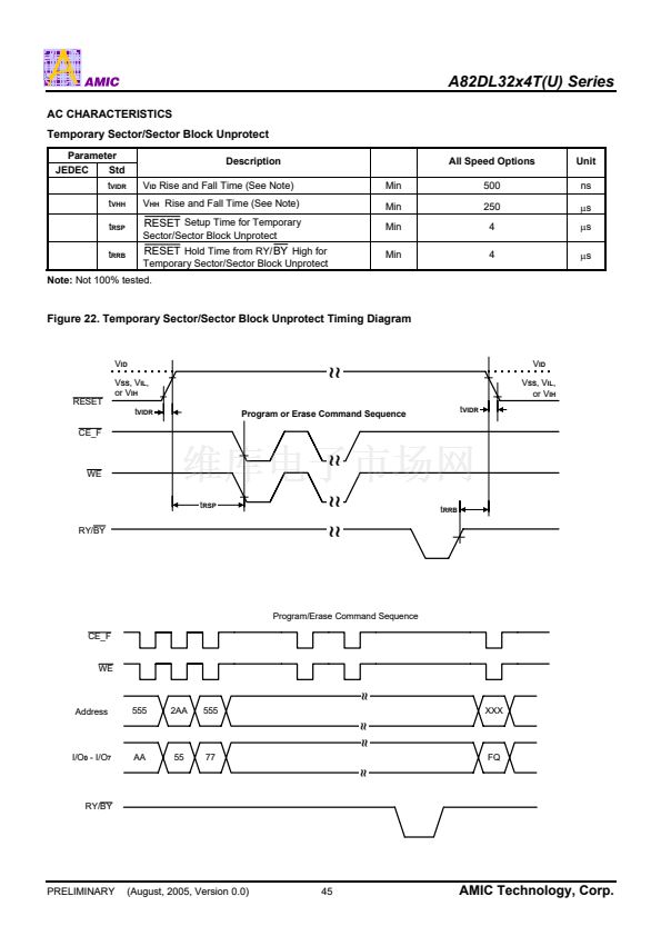
- Temporary Sector Unprotect allows changing data in
protected sectors in-system
Flash Features
ARCHITECTURAL ADVANTAGES
Simultaneous Read/Write operations
- Data can be continuously read from one bank while
executing erase/program functions in other bank
- Zero latency between read and write operations
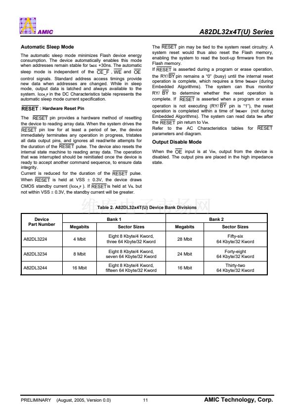
Multiple bank architectures
- Three devices available with different bank sizes (refer to
Table 2)
Package
-
69-Ball TFBGA (8x11x1.4 mm)
Top or bottom boot block
Manufactured on 0.18 碌m process technology
- Compatible with AM42DL32x4G devices
Compatible with JEDEC standards
-
Pinout and software compatible with single-power-supply
flash standard
PERFORMANCE CHARACTERISTICS
High performance
-
Access time as fast as 70ns
-
Program time: 7碌s/word typical utilizing Accelerate
function
Ultra low power consumption (typical values)
-
2mA active read current at 1MHz
-
10mA active read current at 5MHz
-
200nA in standby or automatic sleep mode
Minimum 1 million write cycles guaranteed per sector
20 Year data retention at 125掳C
-
Reliable operation for the life of the system
SOFTWARE FEATURES
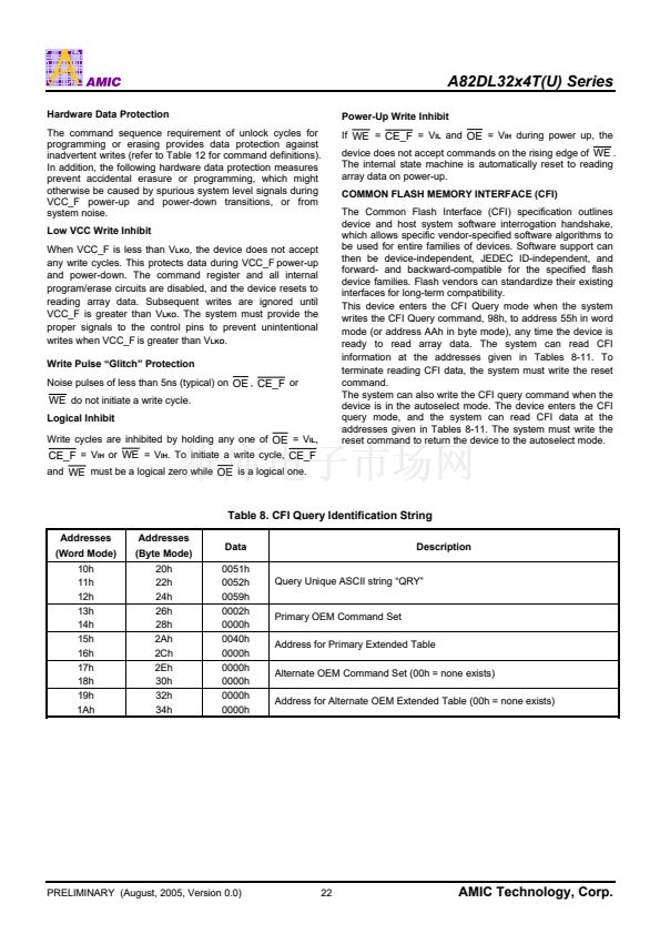
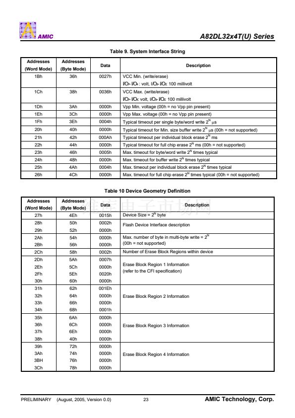
Supports Common Flash Memory Interface (CFI)
Erase Suspend/Erase Resume
LP SRAM Features
Power supply range: 2.7V to 3.6V
Access times: 70 ns (max.)
Current:
Very low power version: Operating: 35mA(max.)
Standby: 10uA (max.)
Full static operation, no clock or refreshing required
All inputs and outputs are directly TTL-compatible
Common I/O using three-state output
Output enable and two chips enable inputs for easy
application
Data retention voltage: 2.0V (min.)
PRELIMINARY (August, 2005, Version 0.0)
1
AMIC Technology, Corp.


 1
1
 2
2
 3
3
 4
4
 5
5
 6
6
 7
7
 8
8
 9
9
 10
10
 11
11
 12
12
 13
13
 14
14
 15
15
 16
16
 17
17
 18
18
 19
19
 20
20
 21
21
 22
22
 23
23
 24
24
 25
25
 26
26
 27
27
 28
28
 29
29
 30
30
 31
31
 32
32
 33
33
 34
34
 35
35
 36
36
 37
37
 38
38
 39
39
 40
40
 41
41
 42
42
 43
43
 44
44
 45
45
 46
46
 47
47
 48
48
 49
49
 50
50
 51
51
 52
52
 53
53
 54
54
 55
55
 56
56
 57
57
 58
58
 59
59
 60
60
