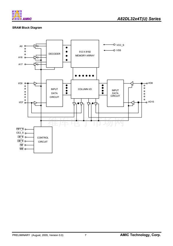
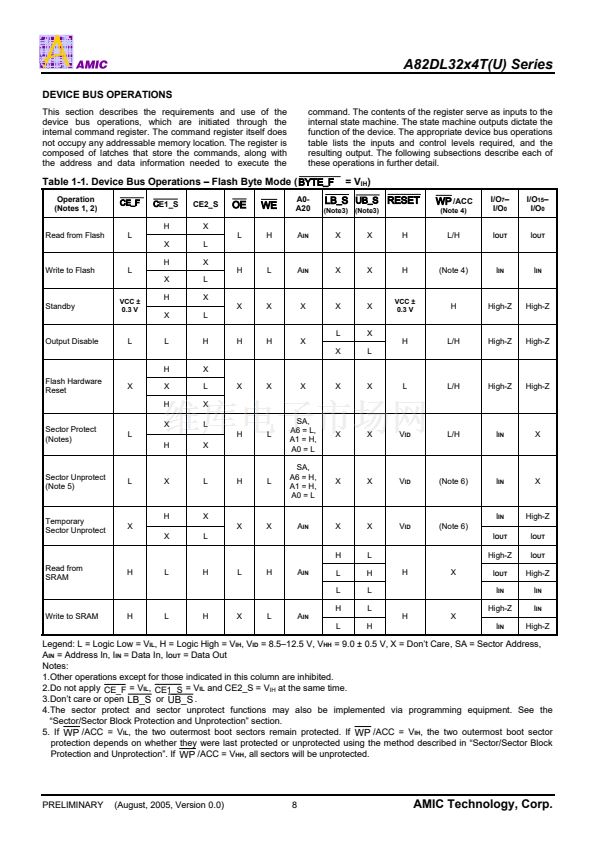
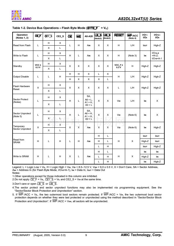
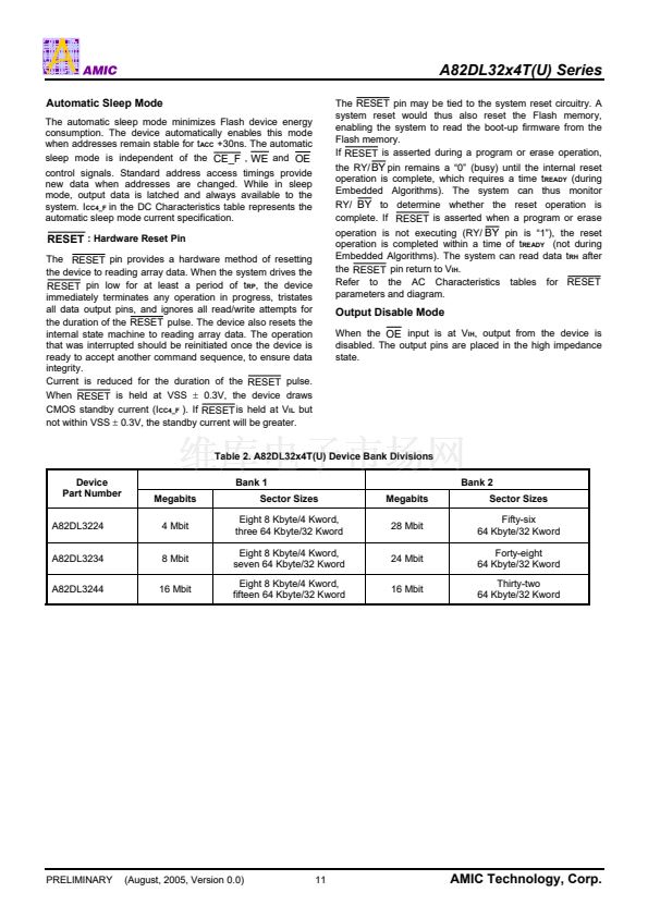
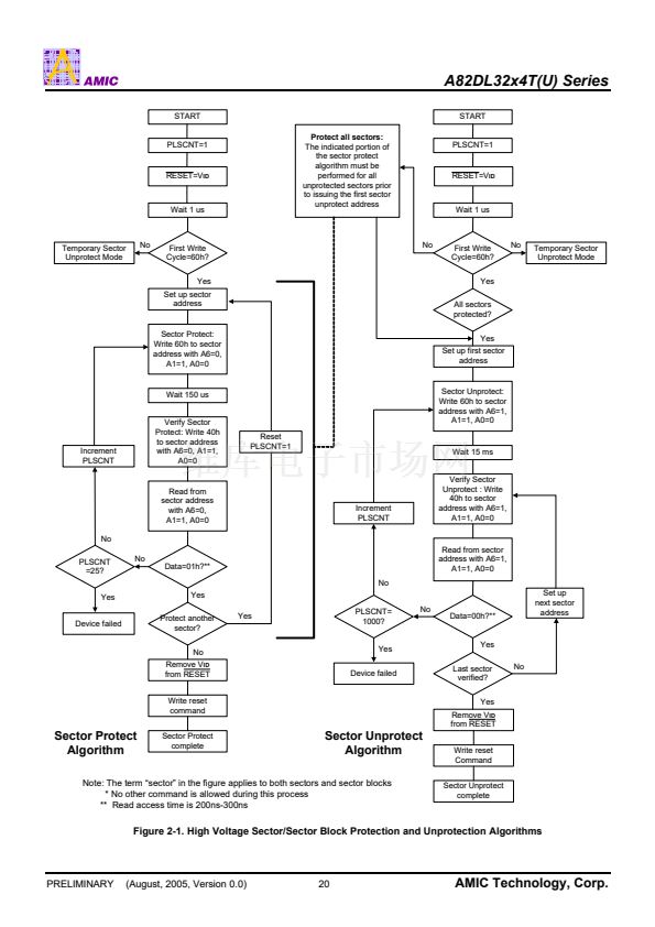
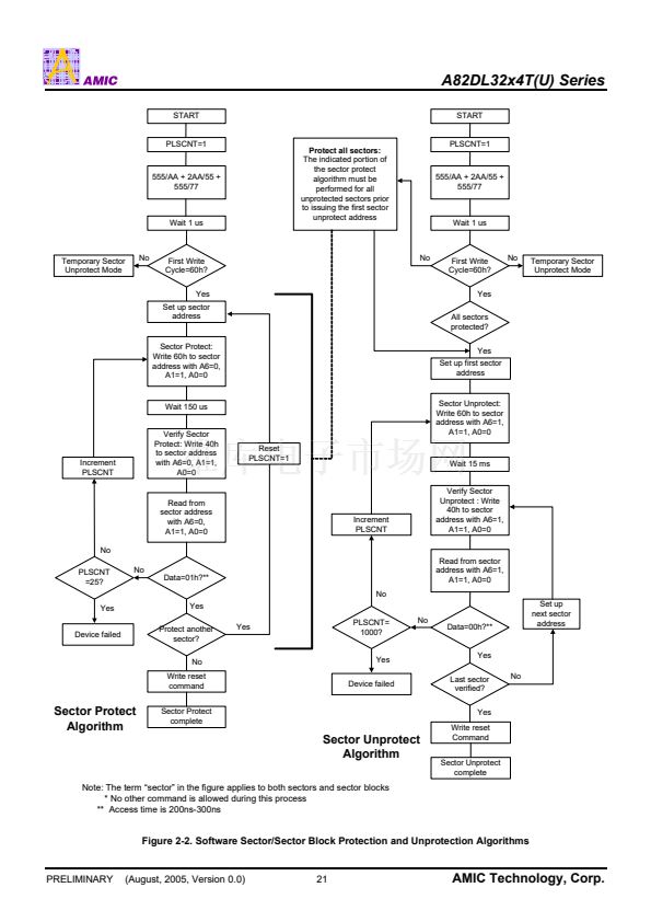
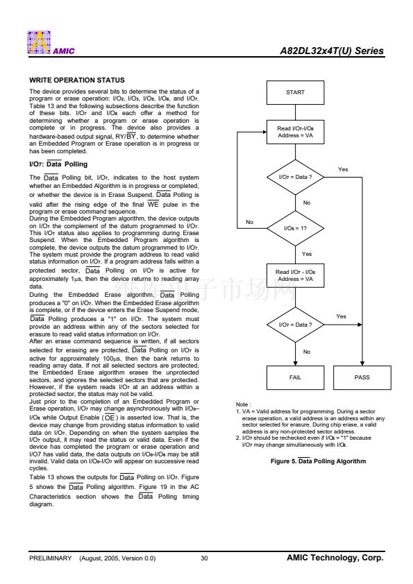
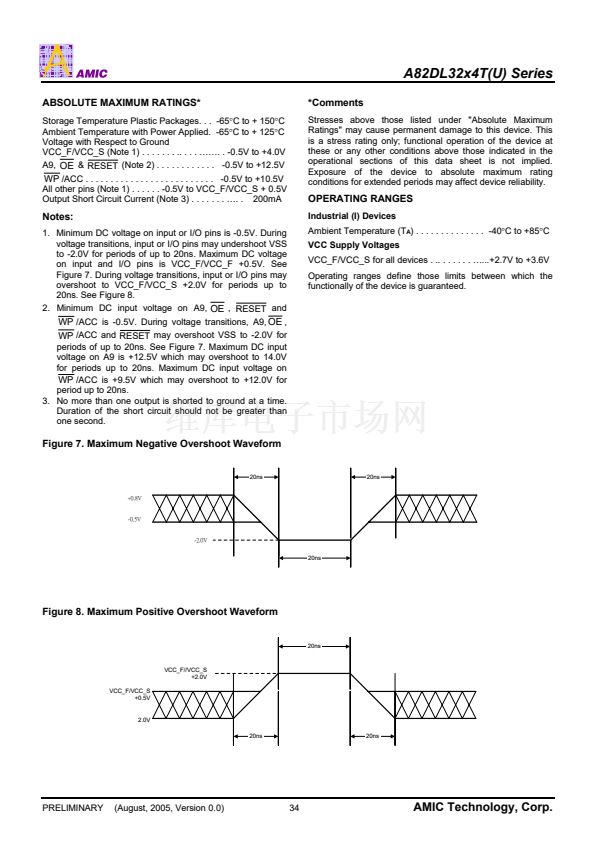
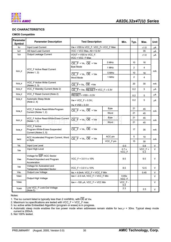
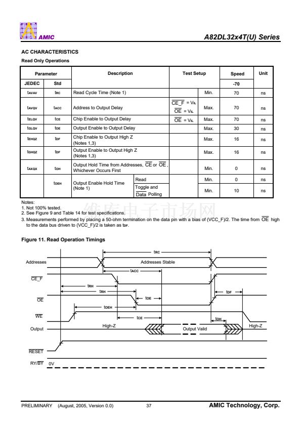
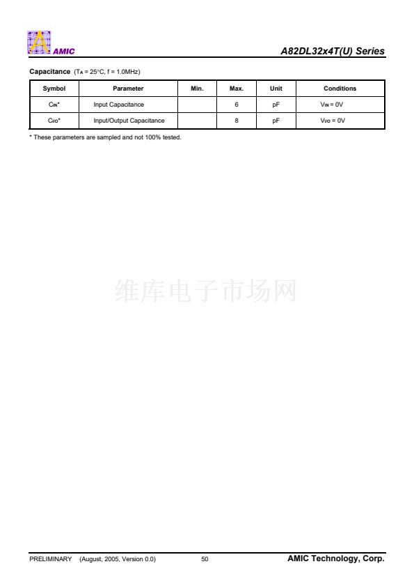
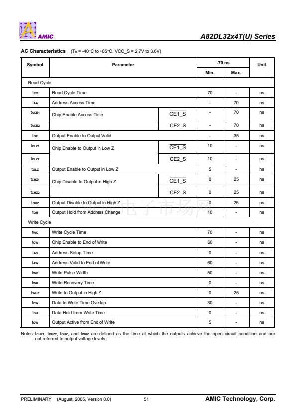
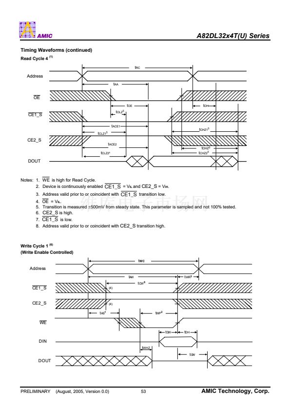
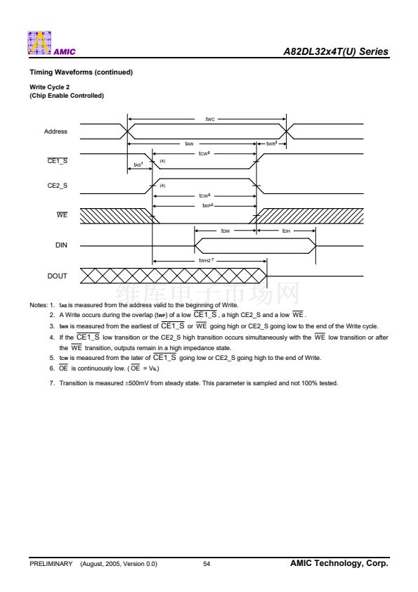
A82DL32x4T(U) Series
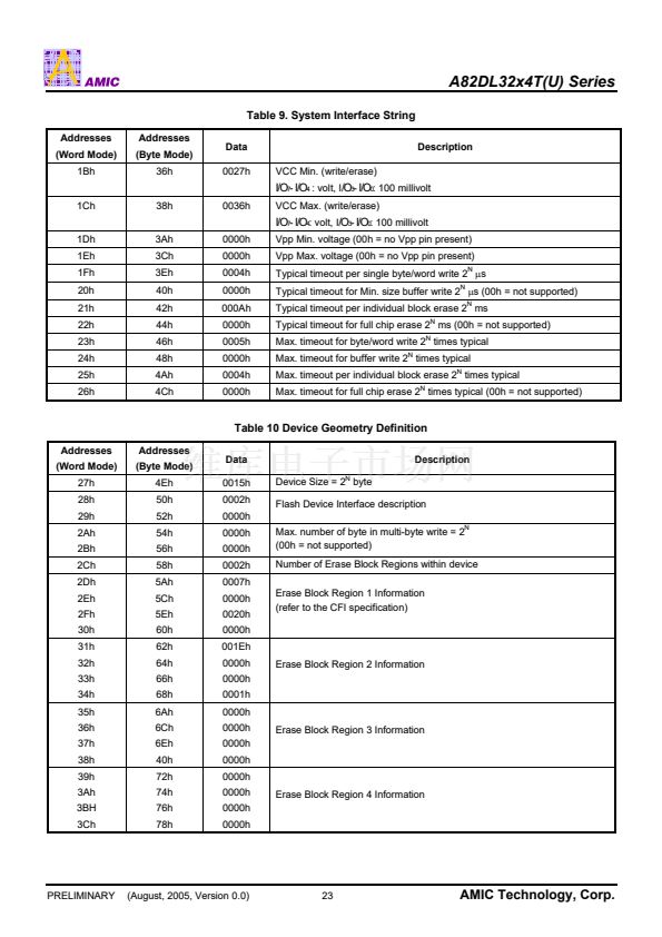
Table 9. System Interface String
Addresses
(Word Mode)
1Bh
1Ch
1Dh
1Eh
1Fh
20h
21h
22h
23h
24h
25h
26h
Addresses
(Byte Mode)
36h
38h
3Ah
3Ch
3Eh
40h
42h
44h
46h
48h
4Ah
4Ch
Data
0027h
0036h
0000h
0000h
0004h
0000h
000Ah
0000h
0005h
0000h
0004h
0000h
VCC Min. (write/erase)
Description
I/O
7
-
I/O
4
: volt, I
/O
3
-
I/O
0
: 100 millivolt
VCC Max. (write/erase)
I/O
7
-
I/O
4
: volt, I
/O
3
-
I/O
0
: 100 millivolt
Vpp Min. voltage (00h = no Vpp pin present)
Vpp Max. voltage (00h = no Vpp pin present)
Typical timeout per single byte/word write 2
N
碌s
Typical timeout for Min. size buffer write 2
N
碌s
(00h = not supported)
Typical timeout per individual block erase 2
N
ms
Typical timeout for full chip erase 2
N
ms (00h = not supported)
Max. timeout for byte/word write 2
N
times typical
Max. timeout for buffer write 2
N
times typical
Max. timeout per individual block erase 2
N
times typical
Max. timeout for full chip erase 2
N
times typical (00h = not supported)
Table 10 Device Geometry Definition
Addresses
(Word Mode)
27h
28h
29h
2Ah
2Bh
2Ch
2Dh
2Eh
2Fh
30h
31h
32h
33h
34h
35h
36h
37h
38h
39h
3Ah
3BH
3Ch
Addresses
(Byte Mode)
4Eh
50h
52h
54h
56h
58h
5Ah
5Ch
5Eh
60h
62h
64h
66h
68h
6Ah
6Ch
6Eh
40h
72h
74h
76h
78h
Data
0015h
0002h
0000h
0000h
0000h
0002h
0007h
0000h
0020h
0000h
001Eh
0000h
0000h
0001h
0000h
0000h
0000h
0000h
0000h
0000h
0000h
0000h
Erase Block Region 4 Information
Erase Block Region 3 Information
Erase Block Region 2 Information
Erase Block Region 1 Information
(refer to the CFI specification)
Max. number of byte in multi-byte write = 2
(00h = not supported)
N
N
Device Size = 2 byte
Description
Flash Device Interface description
Number of Erase Block Regions within device
PRELIMINARY
(August, 2005, Version 0.0)
23
AMIC Technology, Corp.


 1
1
 2
2
 3
3
 4
4
 5
5
 6
6
 7
7
 8
8
 9
9
 10
10
 11
11
 12
12
 13
13
 14
14
 15
15
 16
16
 17
17
 18
18
 19
19
 20
20
 21
21
 22
22
 23
23
 24
24
 25
25
 26
26
 27
27
 28
28
 29
29
 30
30
 31
31
 32
32
 33
33
 34
34
 35
35
 36
36
 37
37
 38
38
 39
39
 40
40
 41
41
 42
42
 43
43
 44
44
 45
45
 46
46
 47
47
 48
48
 49
49
 50
50
 51
51
 52
52
 53
53
 54
54
 55
55
 56
56
 57
57
 58
58
 59
59
 60
60
