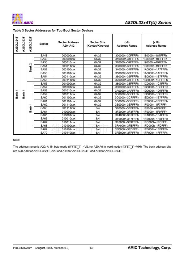
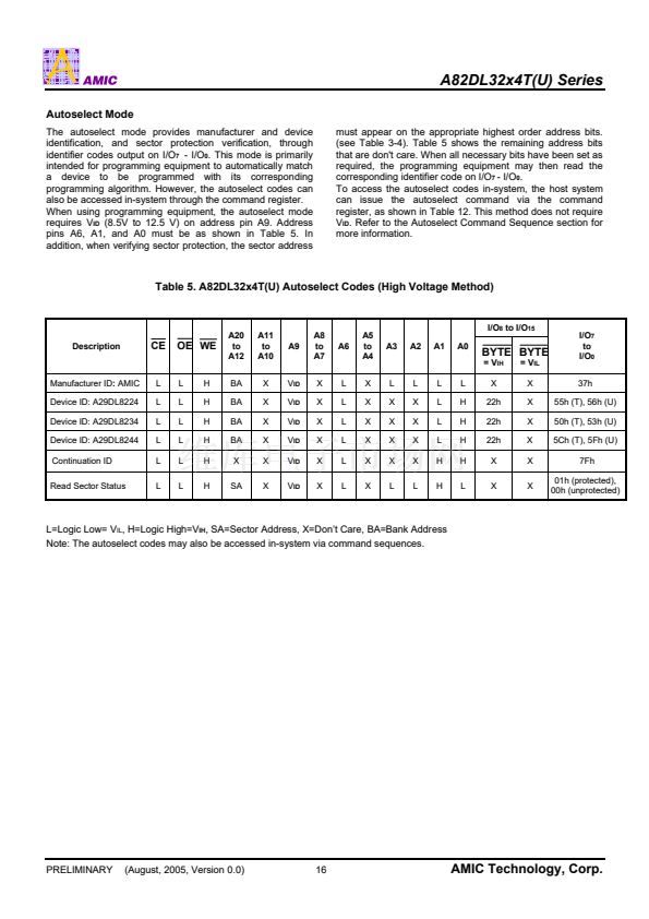
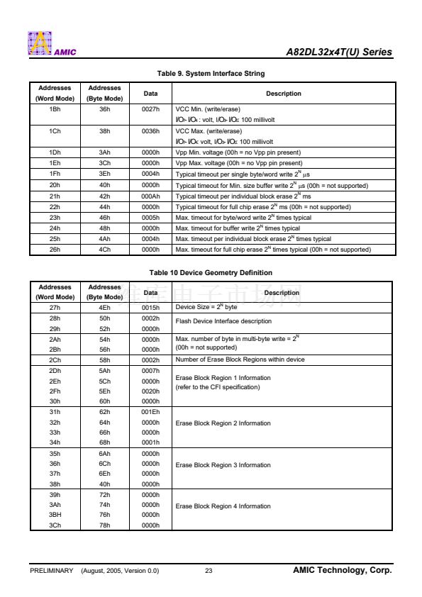
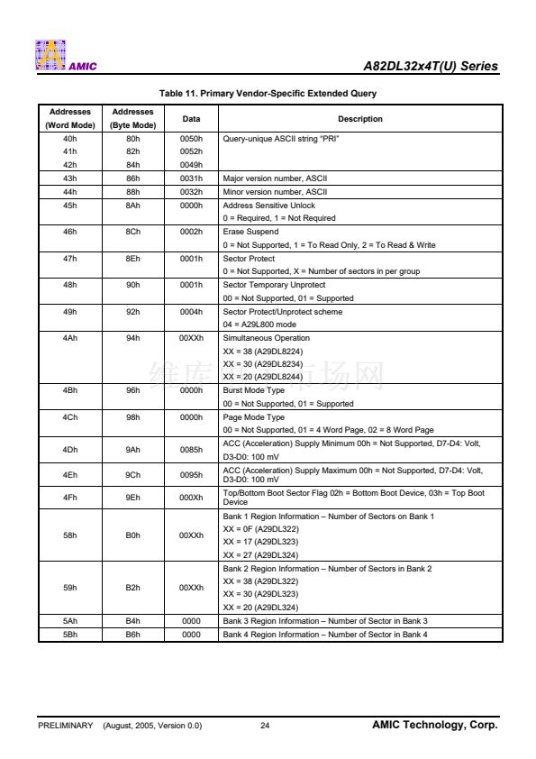
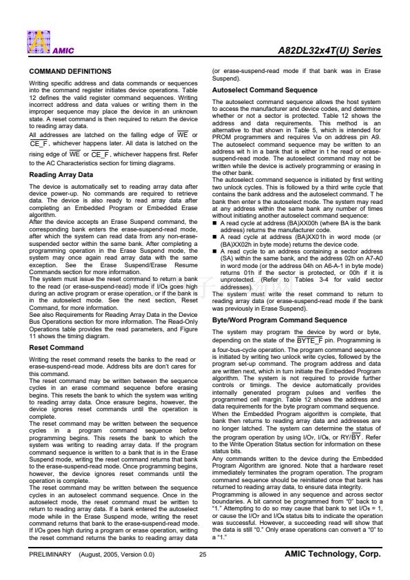
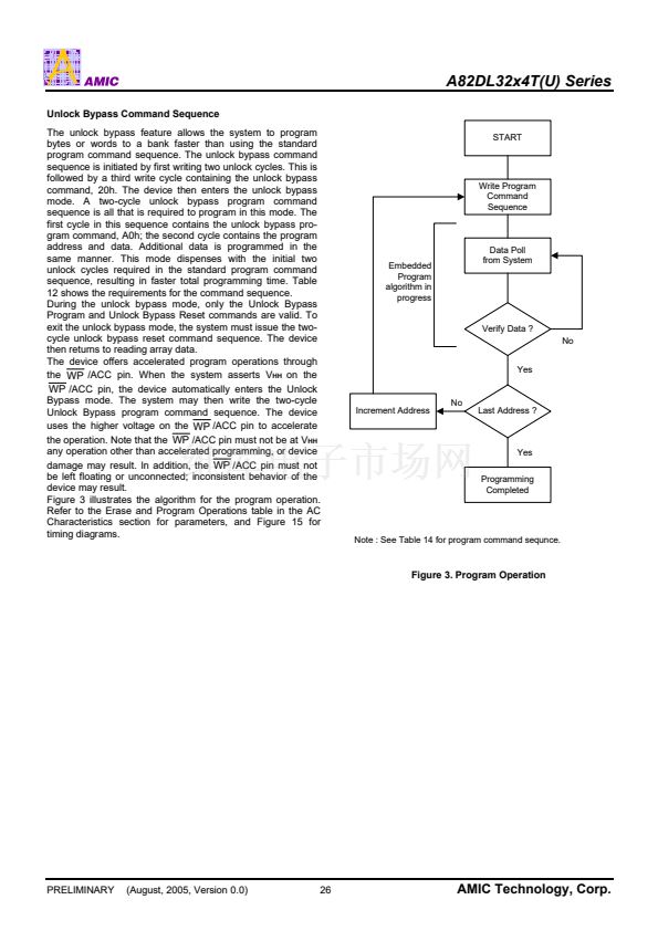
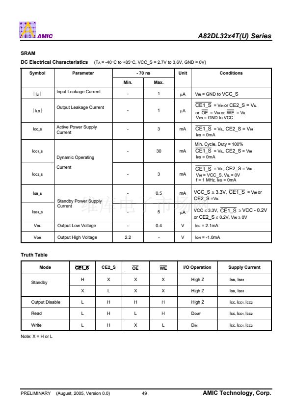
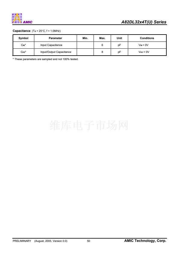
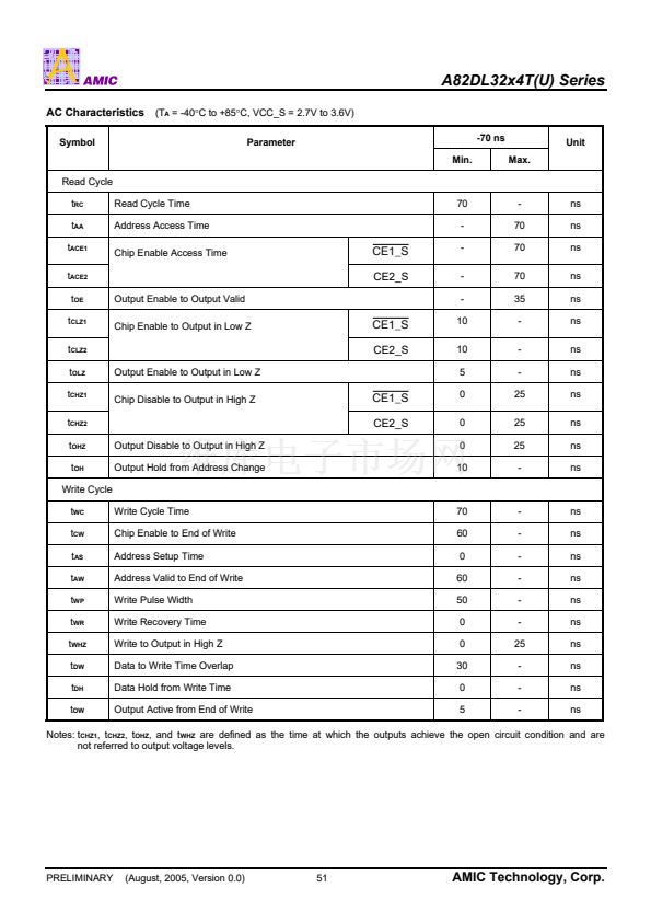
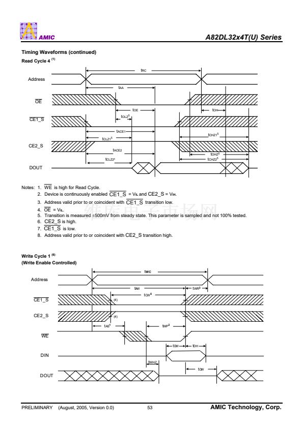
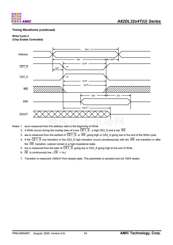
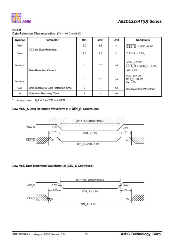
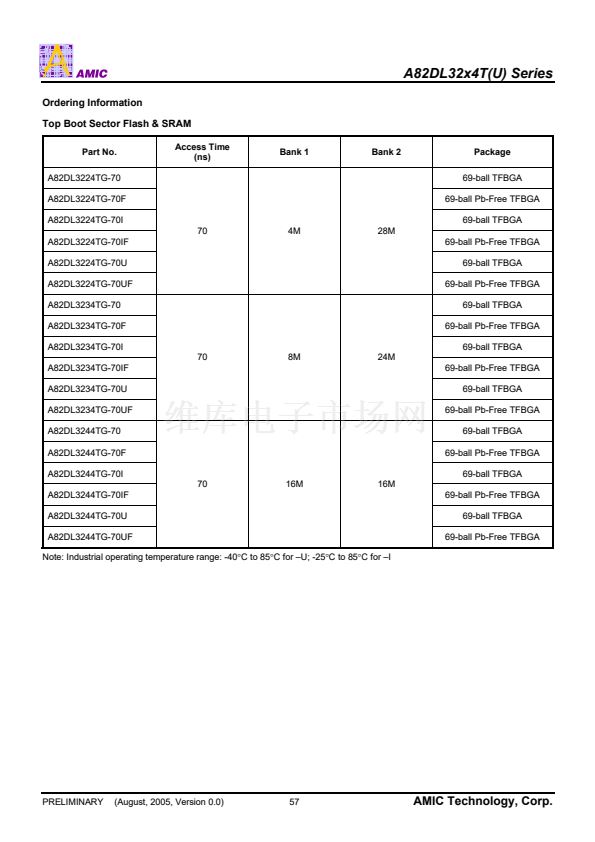
A82DL32x4T(U) Series
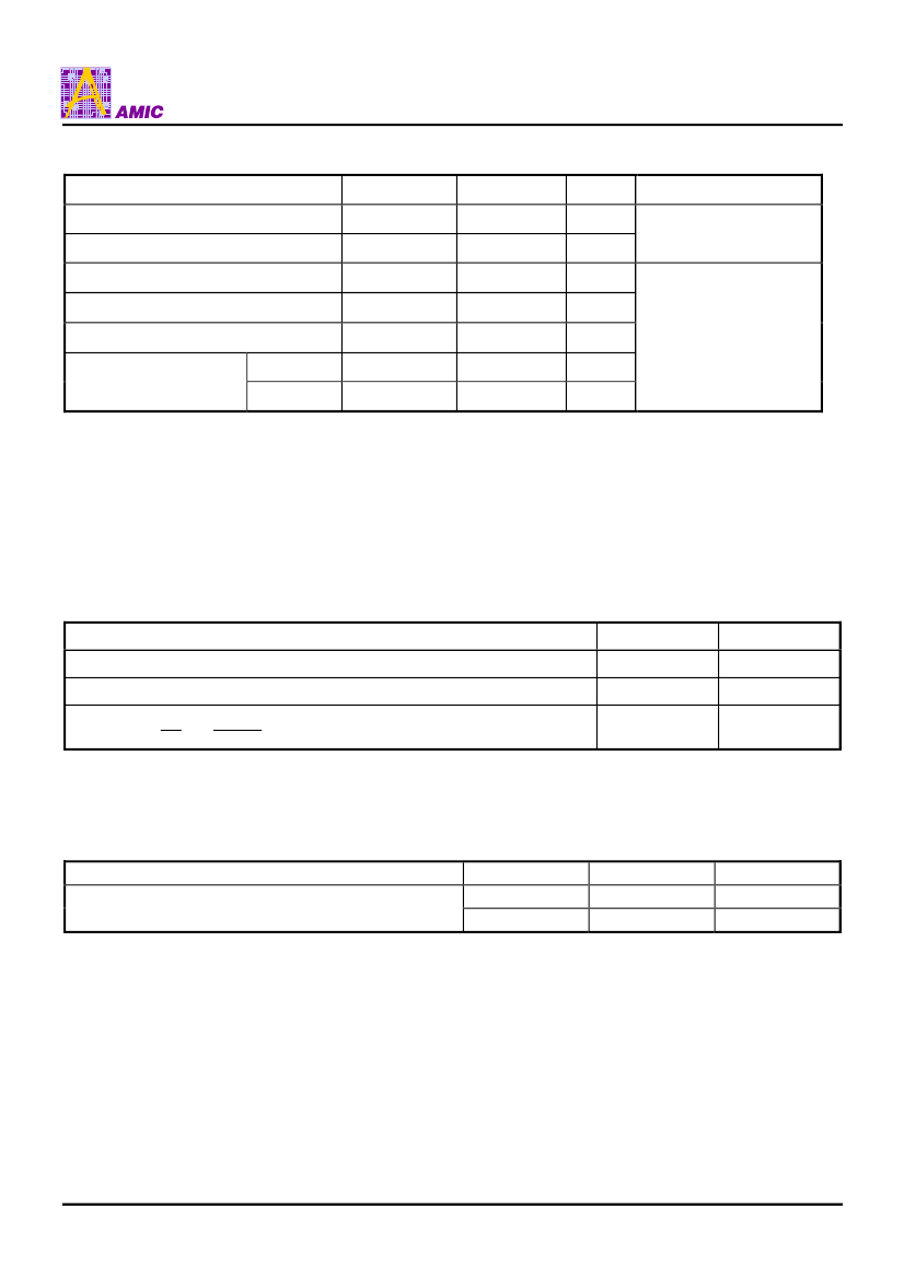
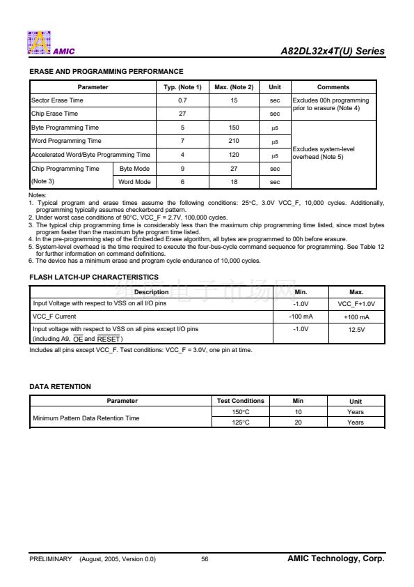
ERASE AND PROGRAMMING PERFORMANCE
Parameter
Sector Erase Time
Chip Erase Time
Byte Programming Time
Word Programming Time
Accelerated Word/Byte Programming Time
Chip Programming Time
(Note 3)
Byte Mode
Word Mode
Typ. (Note 1)
0.7
27
5
7
4
9
6
150
210
120
27
18
Max. (Note 2)
15
Unit
sec
sec
碌
s
碌
s
碌
s
Comments
Excludes 00h programming
prior to erasure (Note 4)
Excludes system-level
overhead (Note 5)
sec
sec
Notes:
1. Typical program and erase times assume the following conditions: 25
掳
C, 3.0V VCC_F, 10,000 cycles. Additionally,
programming typically assumes checkerboard pattern.
2. Under worst case conditions of 90
掳
C, VCC_F = 2.7V, 100,000 cycles.
3. The typical chip programming time is considerably less than the maximum chip programming time listed, since most bytes
program faster than the maximum byte program time listed.
4. In the pre-programming step of the Embedded Erase algorithm, all bytes are programmed to 00h before erasure.
5. System-level overhead is the time required to execute the four-bus-cycle command sequence for programming. See Table 12
for further information on command definitions.
6. The device has a minimum erase and program cycle endurance of 10,000 cycles.
FLASH LATCH-UP CHARACTERISTICS
Description
Input Voltage with respect to VSS on all I/O pins
VCC_F Current
Input voltage with respect to VSS on all pins except I/O pins
(including A9,
OE
and
RESET
)
Includes all pins except VCC_F. Test conditions: VCC_F = 3.0V, one pin at time.
Min.
-1.0V
-100 mA
-1.0V
Max.
VCC_F+1.0V
+100 mA
12.5V
DATA RETENTION
Parameter
Minimum Pattern Data Retention Time
Test Conditions
150
掳
C
125
掳
C
Min
10
20
Unit
Years
Years
PRELIMINARY
(August, 2005, Version 0.0)
56
AMIC Technology, Corp.


 1
1
 2
2
 3
3
 4
4
 5
5
 6
6
 7
7
 8
8
 9
9
 10
10
 11
11
 12
12
 13
13
 14
14
 15
15
 16
16
 17
17
 18
18
 19
19
 20
20
 21
21
 22
22
 23
23
 24
24
 25
25
 26
26
 27
27
 28
28
 29
29
 30
30
 31
31
 32
32
 33
33
 34
34
 35
35
 36
36
 37
37
 38
38
 39
39
 40
40
 41
41
 42
42
 43
43
 44
44
 45
45
 46
46
 47
47
 48
48
 49
49
 50
50
 51
51
 52
52
 53
53
 54
54
 55
55
 56
56
 57
57
 58
58
 59
59
 60
60
