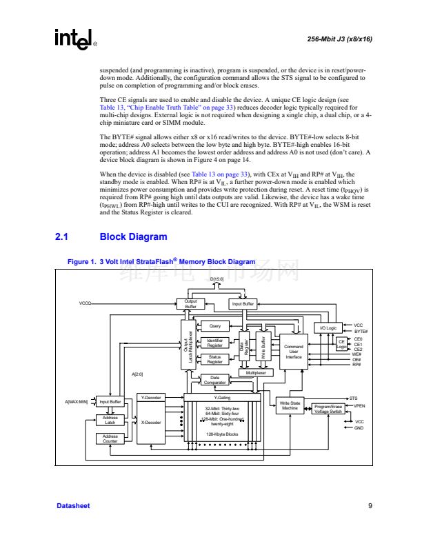
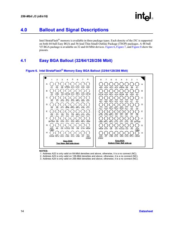
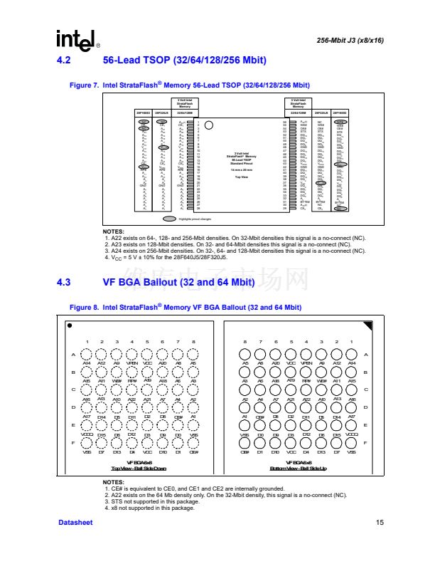
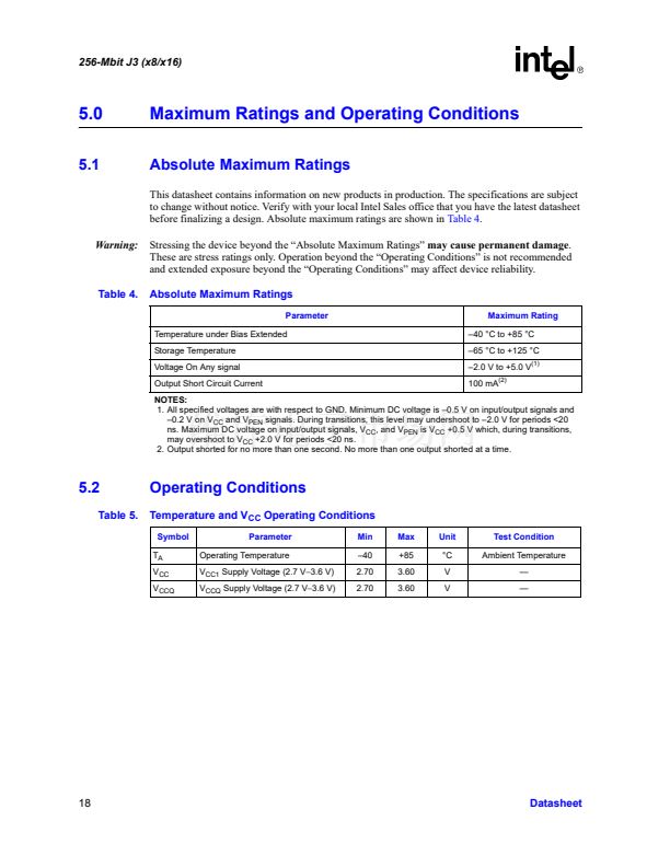
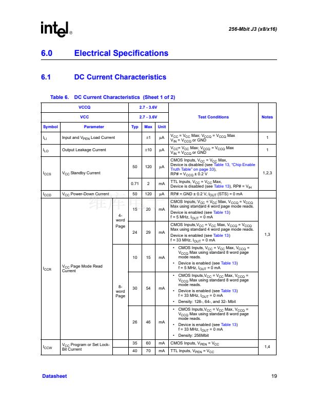
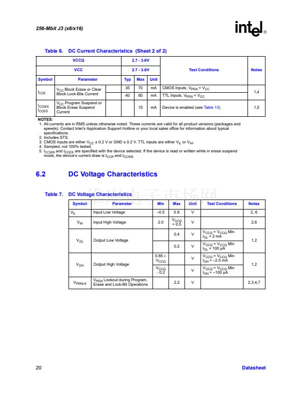
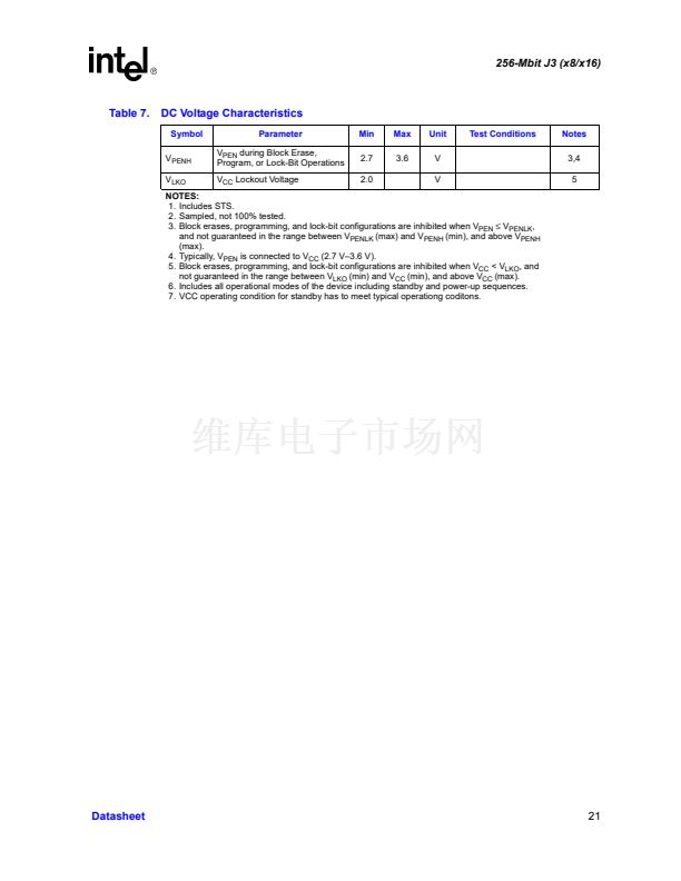
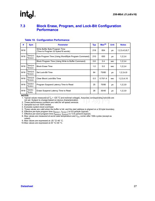
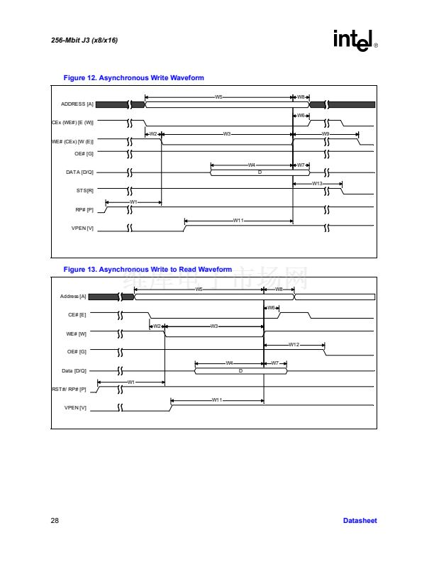
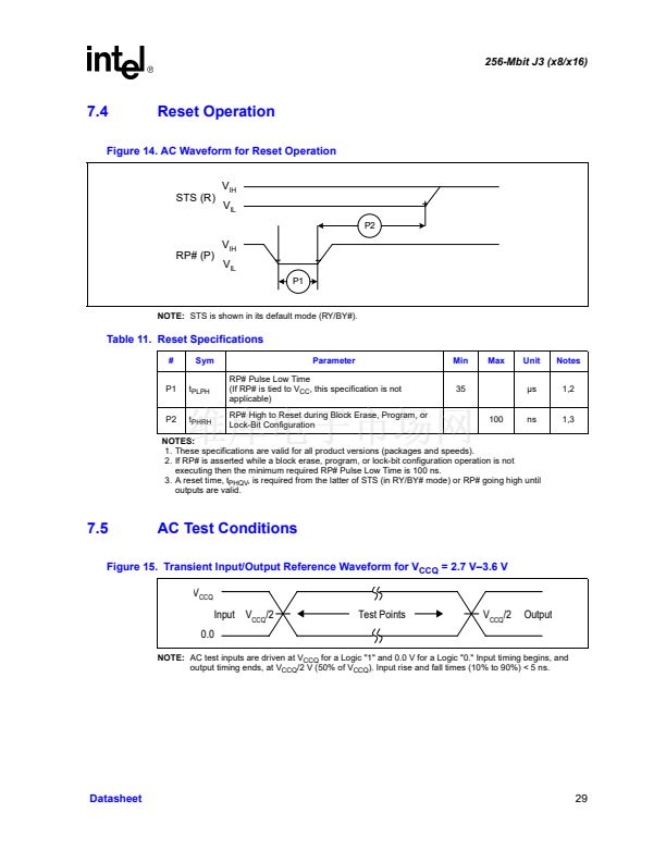
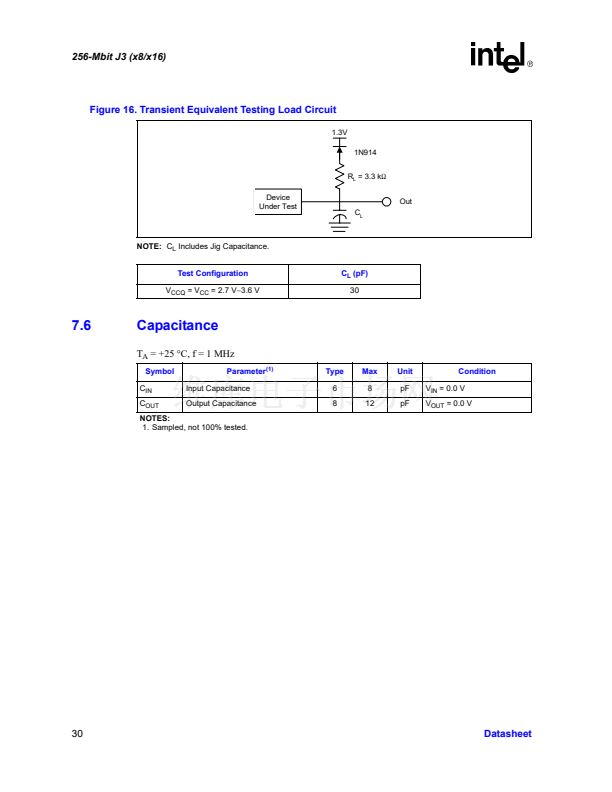
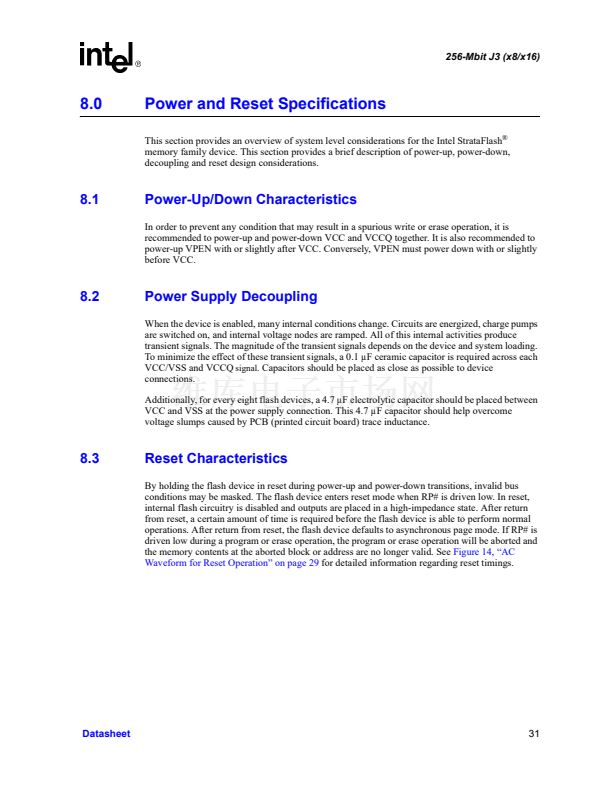
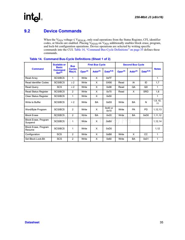
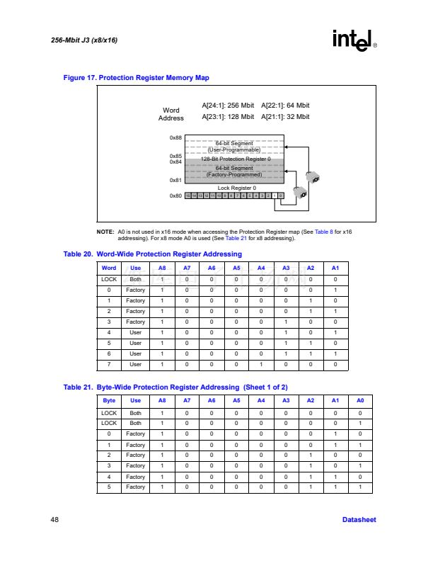
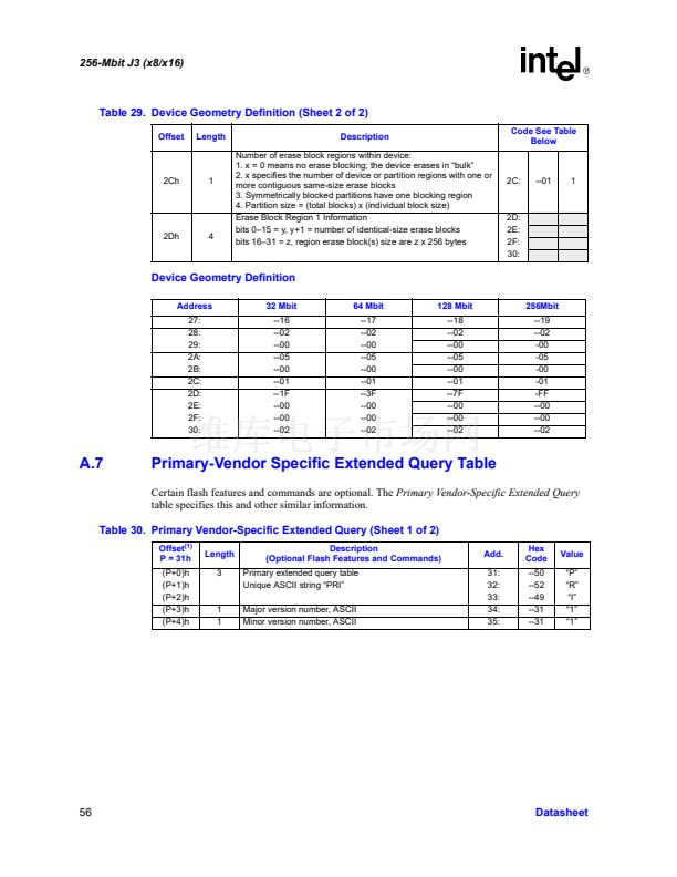
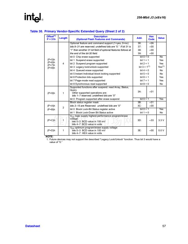
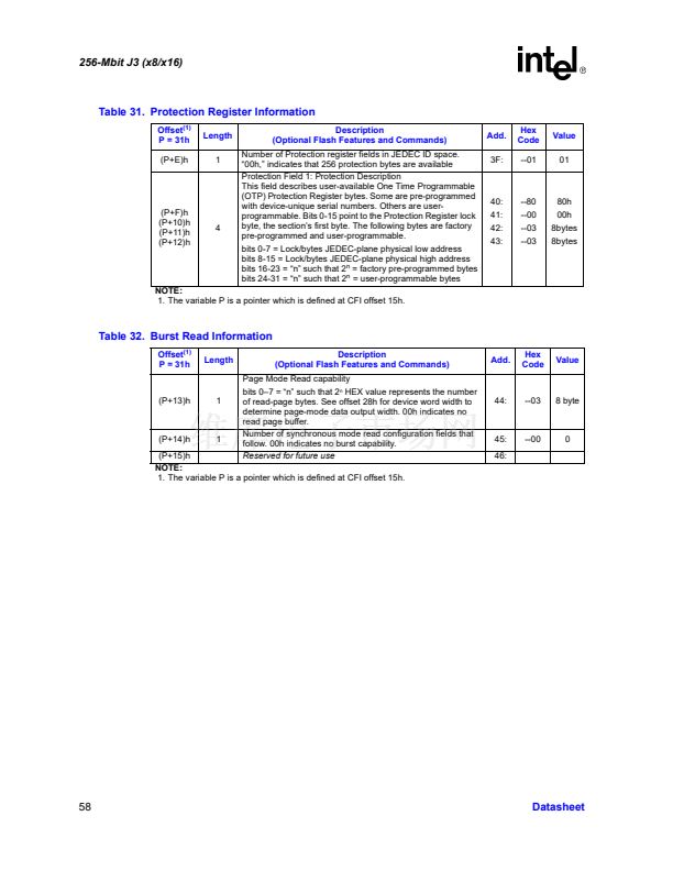
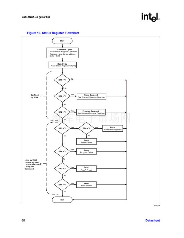
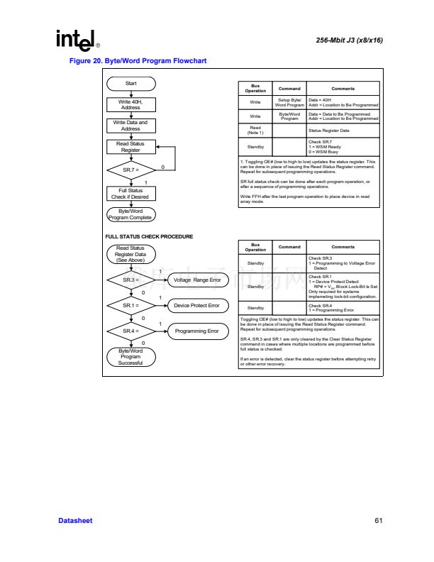
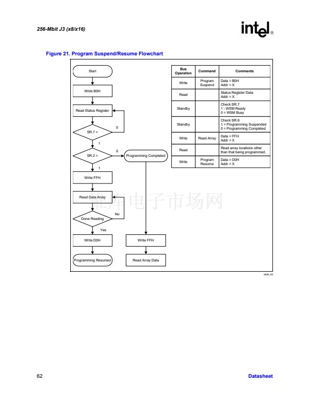
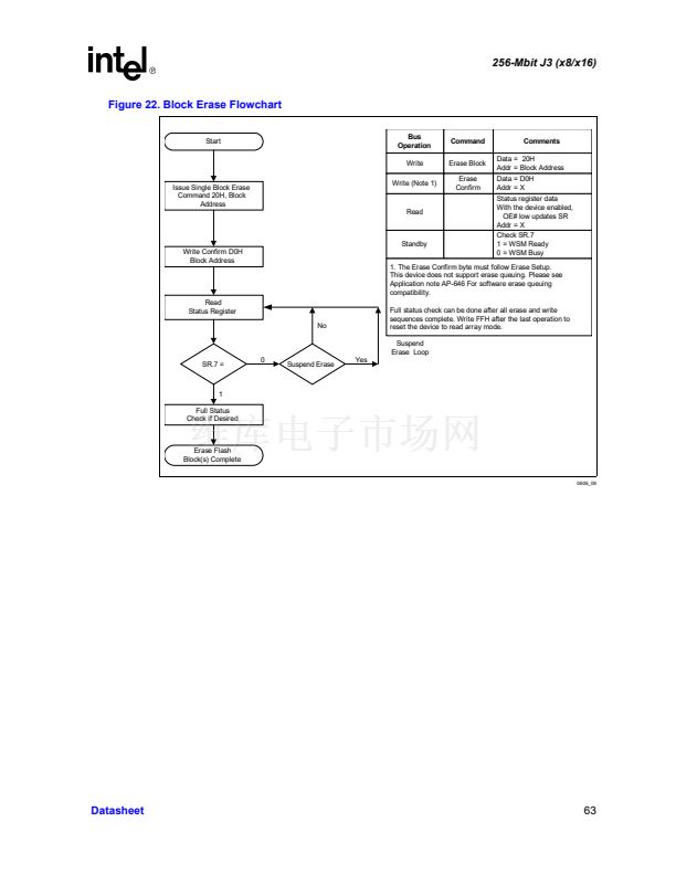
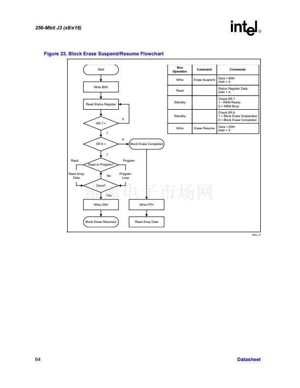
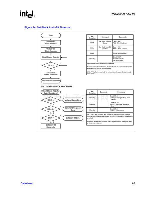
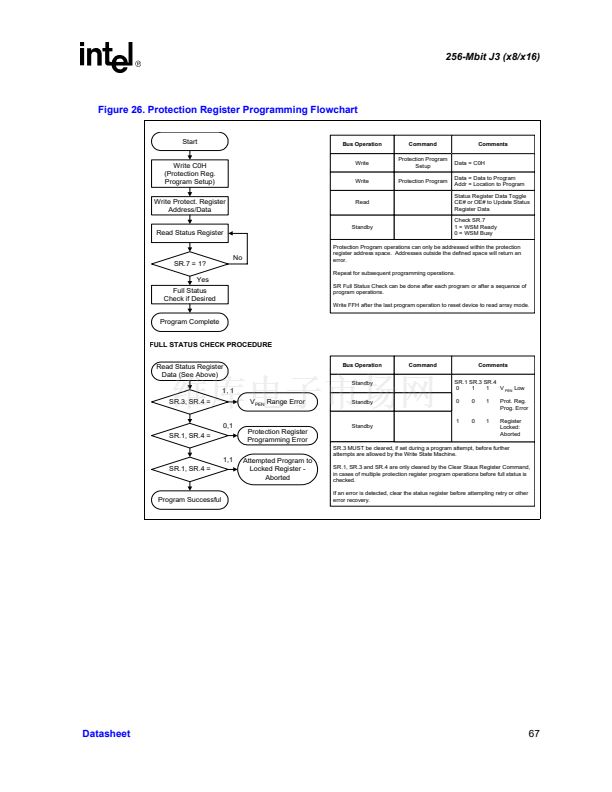
256-Mbit J3 (x8/x16)
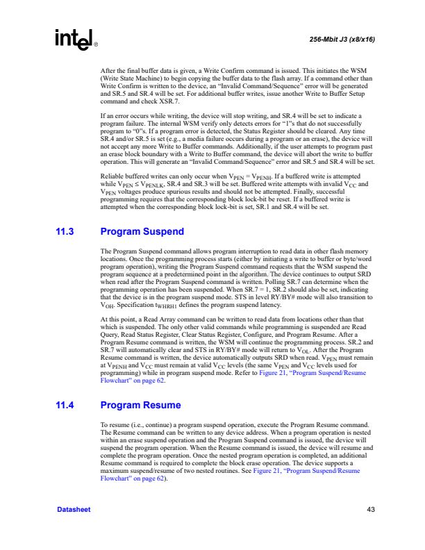
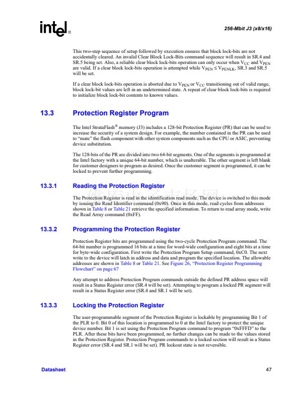
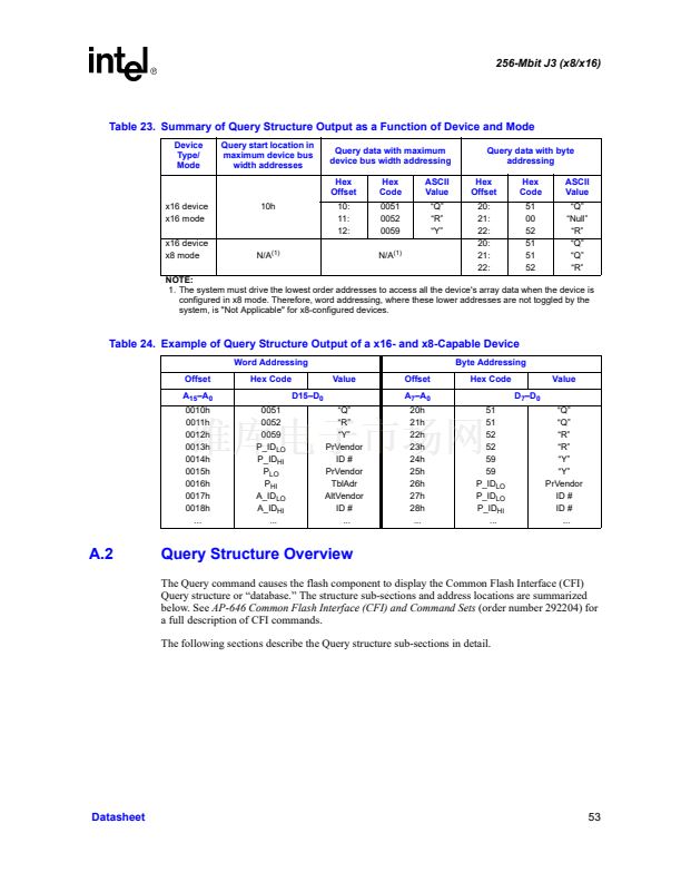
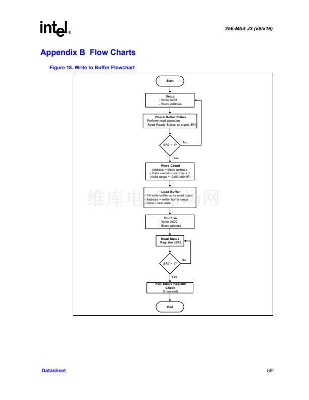
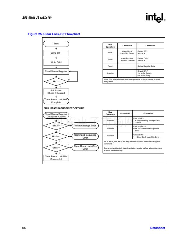
Figure 25. Clear Lock-Bit Flowchart
Start
Bus
Operation
Write
Command
Clear Block
Lock-Bits Setup
Clear Block or
Lock-Bits Confirm
Comments
Data = 60H
Addr = X
Data = D0H
Addr = X
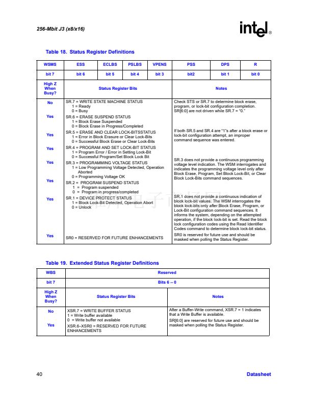
Status Register Data
Check SR.7
1 = WSM Ready
0 = WSM Busy
Write 60H
Write
Write D0H
Read
Read Status Register
Standby
SR.7 =
1
Full Status
Check if Desired
Clear Block Lock-Bits
Complete
0
Write FFH after the clear lock-bits operation to place device in read
array mode.
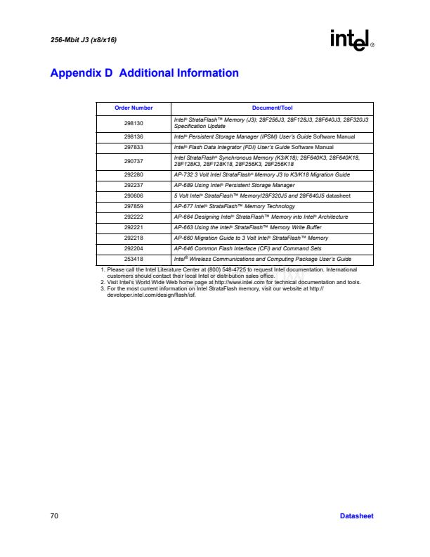
FULL STATUS CHECK PROCEDURE
Read Status Register
Data (See Above)
1
SR.3 =
0
1
SR.4,5 =
0
1
SR.5 =
0
Clear Block Lock-Bits
Successful
Clear Block Lock-Bits
Error
Command Sequence
Error
Voltage Range Error
Standby
Bus
Operation
Standby
Command
Comments
Check SR.3
1 = Programming Voltage Error
Detect
Check SR.4, 5
Both 1 = Command Sequence
Error
Check SR.5
1 = Clear Block Lock-Bits Error
Standby
SR.5, SR.4, and SR.3 are only cleared by the Clear Status Register
command.
If an error is detected, clear the status register before attempting retry
or other error recovery.
66
Datasheet


 1
1
 2
2
 3
3
 4
4
 5
5
 6
6
 7
7
 8
8
 9
9
 10
10
 11
11
 12
12
 13
13
 14
14
 15
15
 16
16
 17
17
 18
18
 19
19
 20
20
 21
21
 22
22
 23
23
 24
24
 25
25
 26
26
 27
27
 28
28
 29
29
 30
30
 31
31
 32
32
 33
33
 34
34
 35
35
 36
36
 37
37
 38
38
 39
39
 40
40
 41
41
 42
42
 43
43
 44
44
 45
45
 46
46
 47
47
 48
48
 49
49
 50
50
 51
51
 52
52
 53
53
 54
54
 55
55
 56
56
 57
57
 58
58
 59
59
 60
60
 61
61
 62
62
 63
63
 64
64
 65
65
 66
66
 67
67
 68
68
 69
69
 70
70
 71
71
 72
72
