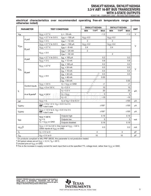
A or B ports鈥?/div>
Ioff
IOZPU
IOZPD
VCC = 3.6 V,
VCC = 0 or 3.6 V,
VCC = 3.6 V
VCC = 0,
VI or VO = 0 to 4.5 V
VCC = 0 to 1.5 V, VO = 0.5 V to 3 V,
OE = don鈥檛 care
VCC = 1.5 V to 0, VO = 0.5 V to 3 V,
OE = don鈥檛 care
VCC = 3.6 V,
IO = 0,
VI = VCC or GND
Outputs high
Outputs low
Outputs disabled
ICC
鈭咺
CC搂
Ci
Cio
VCC = 3 V to 3.6 V, One input at VCC 鈭?0.6 V,
Other inputs at VCC or GND
VI = 3 V or 0
VO = 3 V or 0
* On products compliant to MIL-PRF-38535, this parameter is not production tested.
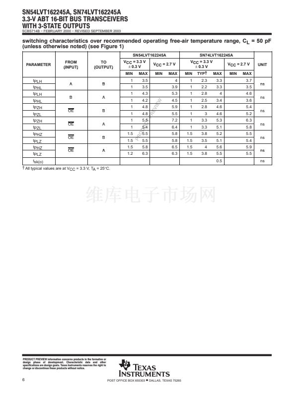
鈥?All typical values are at VCC = 3.3 V, TA = 25掳C.
鈥?Unused pins at VCC or GND.
搂 This is the increase in supply current for each input that is at the specified TTL voltage level, rather than VCC or GND.
PRODUCT PREVIEW information concerns products in the formative or
design phase of development. Characteristic data and other
specifications are design goals. Texas Instruments reserves the right to
change or discontinue these products without notice.
POST OFFICE BOX 655303
鈥?/div>
DALLAS, TEXAS 75265
5


 1
1
 2
2
 3
3
 4
4
 5
5
 6
6
 7
7
 8
8
 9
9
 10
10
 11
11
 12
12
 13
13
 14
14
 15
15
