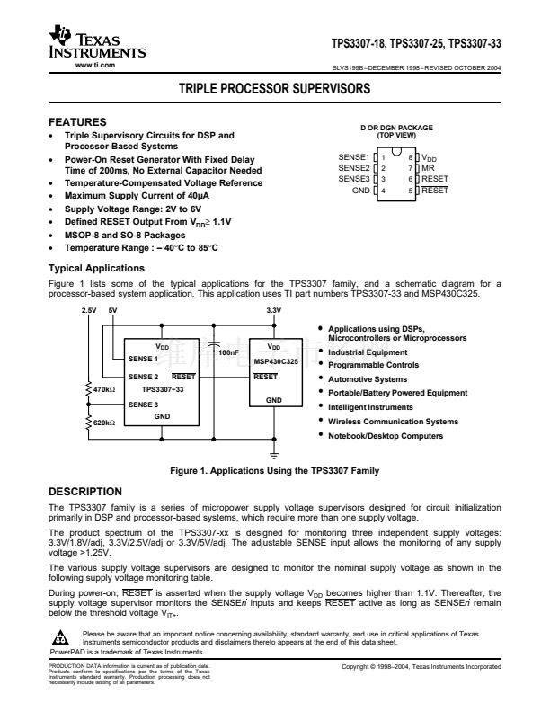
TPS3307-18, TPS3307-25, TPS3307-33
SLVS199B 鈥?DECEMBER 1998 鈥?REVISED OCTOBER 2004
www.ti.com
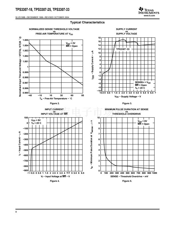
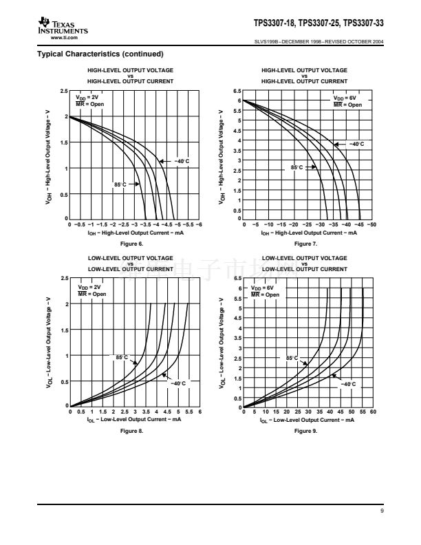
Electrical Characteristics
Over recommended operating free-air temperature range (unless otherwise noted)
PARAMETER
V
OH
High-level output voltage
TEST CONDITIONS
V
DD
= 2V to 6V, I
OH
= -20 碌A
V
DD
= 3.3V, I
OH
= -2mA
V
DD
= 6V, I
OH
= -3mA
V
DD
= 2V to 6V, I
OL
= 20碌A
V
OL
Low-level output voltage
Power-up reset voltage
(1)
VSENSE3
V
DD
= 3.3V, I
OL
= 2mA
V
DD
= 6V, I
OL
= 3mA
V
DD
鈮?/div>
1.1V, I
OL
= 20碌A
V
DD
= 2V to 6V, T
A
= 0掳C to 85掳C
1.22
1.64
VSENSE1,
VSENSE2
V
IT-
Negative-going input threshold volt-
age
(2)
2.20
2.86
4.46
VSENSE3
V
DD
= 2V to 6V,
T
A
= -40掳C to 85掳C
1.22
1.64
VSENSE1,
VSENSE2
2.20
2.86
4.46
V
IT-
= 1.25V
V
IT-
= 1.68V
V
hys
Hysteresis at VSENSEn input
V
IT-
= 2.25V
V
IT-
= 2.93V
V
IT-
= 4.55V
MR
I
H
High-level input current
SENSE1
SENSE2
SENSE3
I
L
I
DD
C
i
(1)
(2)
Low-level input current
Supply current
Input capacitance
V
I
= 0V to V
DD
10
MR
SENSEn
MR = 0.7
脳
V
DD,
V
DD
= 6 V
VSENSE1 = V
DD
= 6V
VSENSE2 = V
DD
= 6V
VSENSE3 = V
DD
MR = 0V, V
DD
= 6V
VSENSE1,2,3 = 0V
-25
-25
-430
1.25
1.68
2.25
2.93
4.55
1.25
1.68
2.25
2.93
4.55
10
15
20
30
40
-130
5
6
-180
8
9
25
-600
25
40
nA
碌A
nA
碌A
pF
碌A
mV
MIN
V
DD
- 0.2V
V
DD
- 0.4V
V
DD
- 0.4V
0.2
0.4
0.4
0.4
1.28
1.72
2.30
3
4.64
1.29
1.73
2.32
3.02
4.67
V
V
V
V
V
V
TYP
MAX
UNIT
The lowest supply voltage at which RESET becomes active. t
r
, V
DD
鈮?/div>
15碌s/V
To ensure best stability of the threshold voltage, a bypass capacitor (ceramic 0.1碌F) should be placed close to the supply terminals.
6


 1
1
 2
2
 3
3
 4
4
 5
5
 6
6
 7
7
 8
8
 9
9
 10
10
 11
11
 12
12
 13
13
 14
14
