TPS3307-18, TPS3307-25, TPS3307-33
www.ti.com
SLVS199B 鈥?DECEMBER 1998 鈥?REVISED OCTOBER 2004
Absolute Maximum Ratings
(1)
Over operating free-air temperature range (unless otherwise noted).
UNIT
Supply voltage, V
DD (2)
All other
pins
(2)
Maximum low output current, I
OL
Maximum high output current, I
OH
Input clamp current, I
IK
(V
I
< 0 or V
I
> V
DD
)
Output clamp current, I
OK
(V
O
< 0 or V
O
> V
DD
)
Continuous total power dissipation
Operating free-air temperature range, T
A
Storage temperature range, T
stg
Soldering temperature
(1)
(2)
7V
-0.3V to 7V
5mA
-5mA
卤20mA
卤20mA
See Dissipation Rating Table
-40掳C to 85掳C
-65掳C to 150掳C
260掳C
Stresses beyond those listed under absolute maximum ratings may cause permanent damage to the device. These are stress ratings
only, and functional operation of the device at these or any other conditions beyond those indicated under recommended operating
conditions is not implied. Exposure to absolute-maximum-rated conditions for extended periods may affect device reliability.
All voltage values are with respect to GND. For reliable operation the device must not be operated at 7V for more than t = 1000h
continuously.
Dissipation Rating Table
PACKAGE
DGN
D
T
A
鈮?/div>
25掳C
POWER RATING
2.14W
725mW
DERATING FACTOR
ABOVE T
A
= 25掳C
17.1mW/掳C
5.8mW/掳C
T
A
= 70掳C
POWER RATING
1.37W
464mW
T
A
= 85掳C
POWER RATING
1.11W
377mW
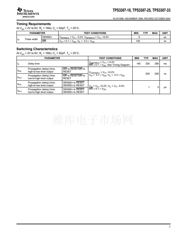
Recommended Operating Conditions
At specified temperature range.
MIN
Supply voltage, V
DD
Input voltage at MR and SENSE3, V
I
Input voltage at SENSE1 and SENSE2, V
I
High-level input voltage at MR, V
IH
Low-level input voltage at MR, V
IL
Input transition rise and fall rate at MR,
鈭唗/鈭哣
Operating free-air temperature range, T
A
-40
2
0
0
0.7 x V
DD
0.3
脳
V
DD
50
85
MAX
6
V
DD
+ 0.3
(V
DD
+0.3)V
IT
/1.25V
UNIT
V
V
V
V
V
ns/V
掳C
5


 1
1
 2
2
 3
3
 4
4
 5
5
 6
6
 7
7
 8
8
 9
9
 10
10
 11
11
 12
12
 13
13
 14
14
