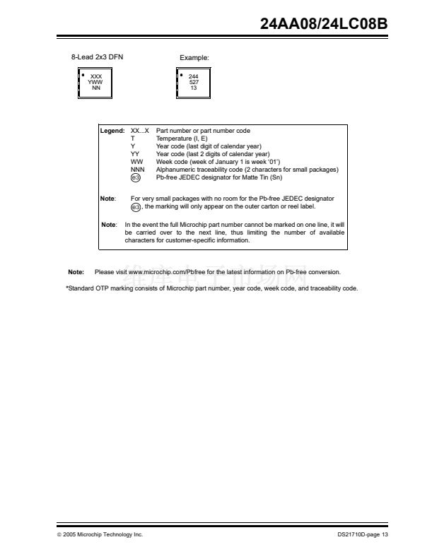
鈥?/div>
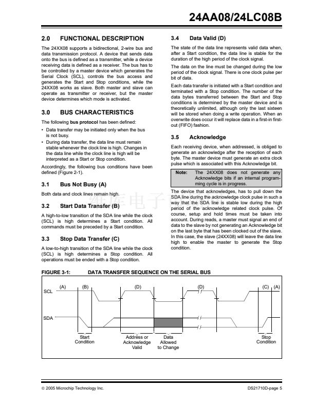
2
3
1
5
4
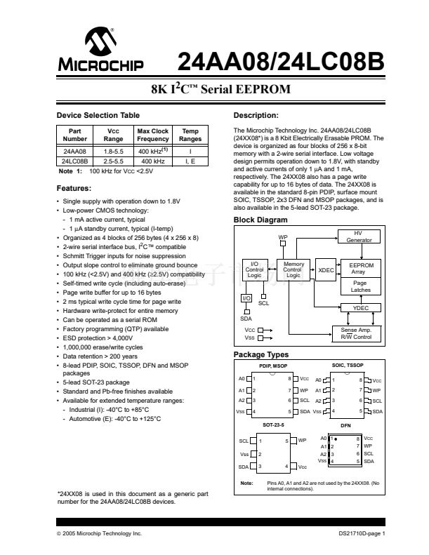
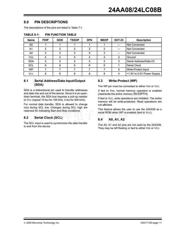
Description
Not Connected
Not Connected
Not Connected
Ground
Serial Address/Data I/O
Serial Clock
Write-Protect Input
+1.8V to 5.5V Power Supply
8.1
Serial Address/Data Input/Output
(SDA)
8.3
Write-Protect (WP)
The WP pin must be connected to either V
SS
or V
CC
.
If tied to V
SS
, normal memory operation is enabled
(read/write the entire memory
00-03FFH
).
If tied to V
CC
, write operations are inhibited. The entire
memory will be write-protected. Read operations are
not affected.
This feature allows the user to use the 24XX08 as a
serial ROM when WP is enabled (tied to V
CC
).
SDA is a bidirectional pin used to transfer addresses
and data into and out of the device. Since it is an open-
drain terminal, the SDA bus requires a pull-up resistor
to V
CC
(typical 10 k惟 for 100 kHz, 2 k惟 for 400 kHz).
For normal data transfer, SDA is allowed to change
only during SCL low. Changes during SCL high are
reserved for indicating Start and Stop conditions.
8.2
Serial Clock (SCL)
8.4
A0, A1, A2
The SCL input is used to synchronize the data transfer
to and from the device.
The A0, A1 and A2 pins are not used by the 24XX08.
They may be left floating or tied to either V
SS
or V
CC
.
漏
2005 Microchip Technology Inc.
DS21710D-page 11


 1
1
 2
2
 3
3
 4
4
 5
5
 6
6
 7
7
 8
8
 9
9
 10
10
 11
11
 12
12
 13
13
 14
14
 15
15
 16
16
 17
17
 18
18
 19
19
 20
20
 21
21
 22
22
 23
23
 24
24
 25
25
 26
26
