TABLE OF CONTENTS
Product Selector Guide . . . . . . . . . . . . . . . . . . . . .
Block Diagram . . . . . . . . . . . . . . . . . . . . . . . . . . . .
Connection Diagrams . . . . . . . . . . . . . . . . . . . . . .
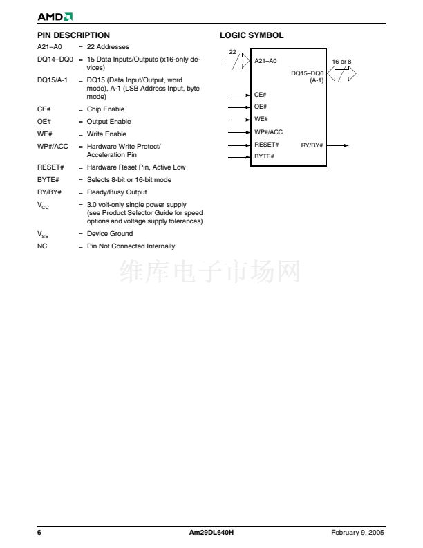
Pin Description. . . . . . . . . . . . . . . . . . . . . . . . . . . .
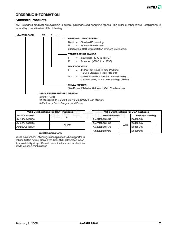
Ordering Information . . . . . . . . . . . . . . . . . . . . . . .
Device Bus Operations . . . . . . . . . . . . . . . . . . . . .
4
4
5
6
7
8
DQ6: Toggle Bit I .................................................................... 29
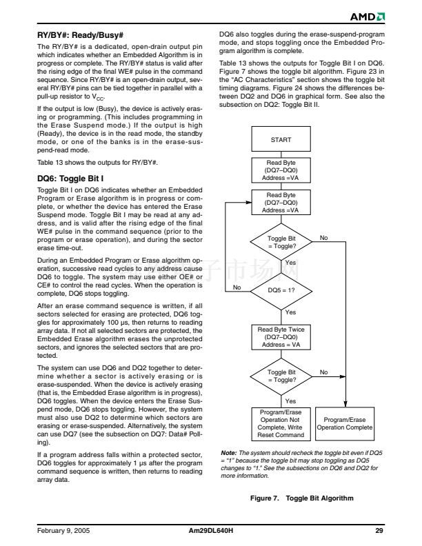
Figure 7. Toggle Bit Algorithm........................................................ 29
DQ2: Toggle Bit II ................................................................... 30
Reading Toggle Bits DQ6/DQ2 ............................................... 30
DQ5: Exceeded Timing Limits ................................................ 30
DQ3: Sector Erase Timer ....................................................... 30
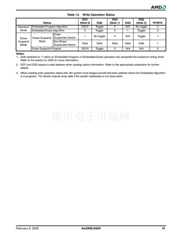
Table 13. Write Operation Status ................................................... 31
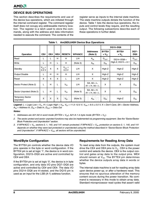
Table 1. Am29DL640H Device Bus Operations ................................8
Requirements for Reading Array Data ..................................... 8
Writing Commands/Command Sequences .............................. 9
Accelerated Program Operation ............................................... 9
Autoselect Functions ................................................................ 9
Simultaneous Read/Write Operations with Zero Latency ......... 9
Automatic Sleep Mode ........................................................... 10
RESET#: Hardware Reset Pin ............................................... 10
Output Disable Mode .............................................................. 10
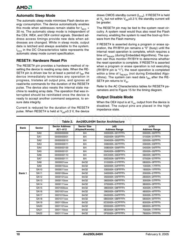
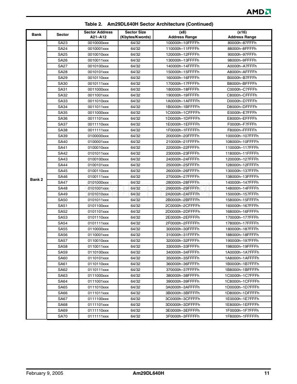
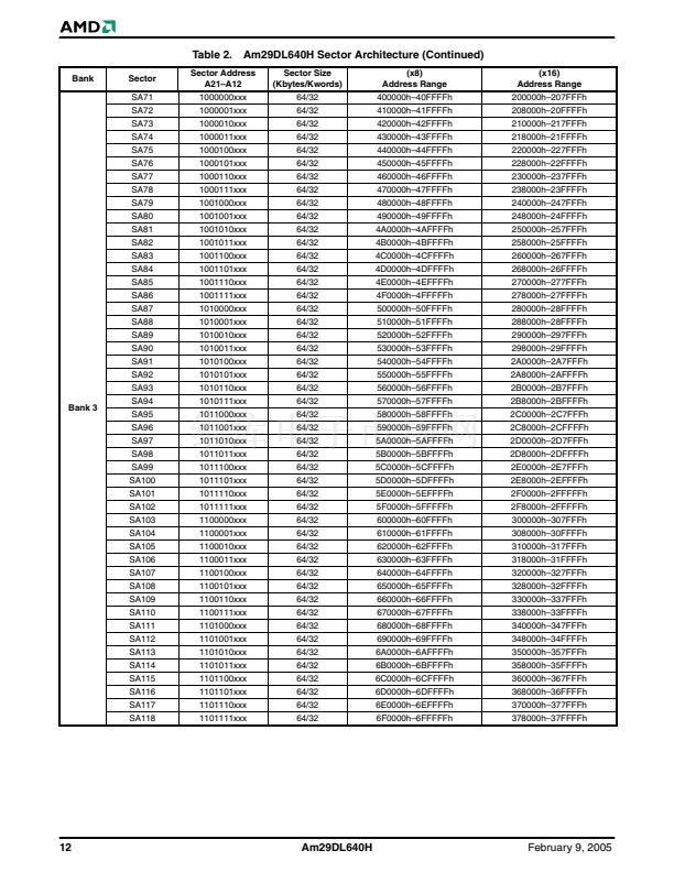
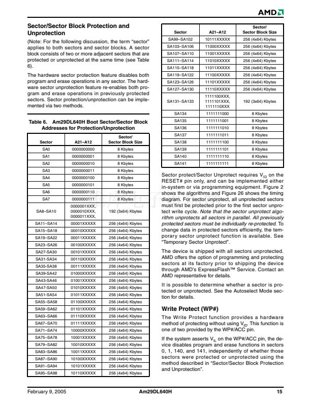
Table 2. Am29DL640H Sector Architecture ....................................10
Table 3. Bank Address ....................................................................13
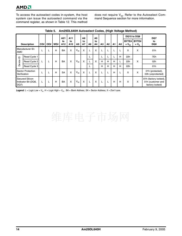
Table 5. Am29DL640H Autoselect Codes, (High Voltage Method) 14
Table 6. Am29DL640H Boot Sector/Sector Block Addresses for
Protection/Unprotection ...................................................................15
Absolute Maximum Ratings. . . . . . . . . . . . . . . . . 32
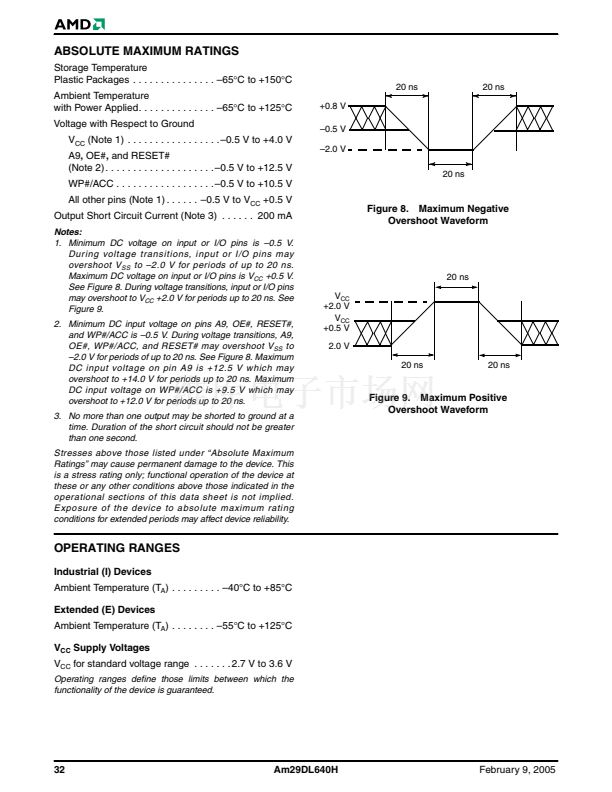
Figure 8. Maximum Negative Overshoot Waveform ...................... 32
Figure 9. Maximum Positive Overshoot Waveform........................ 32
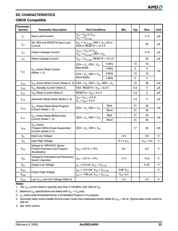
DC Characteristics . . . . . . . . . . . . . . . . . . . . . . . . 33
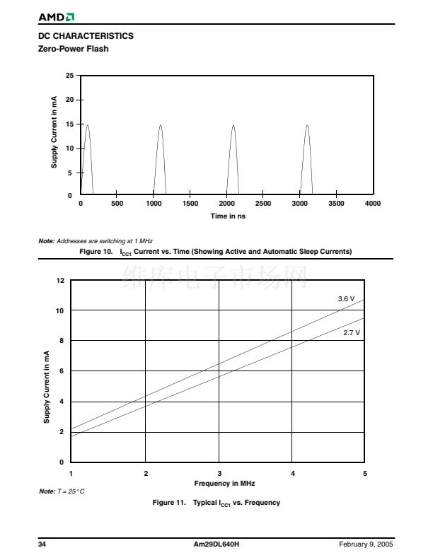
Figure 10. I
CC1
Current vs. Time (Showing Active and
Automatic Sleep Currents) ............................................................. 34
Figure 11. Typical I
CC1
vs. Frequency ............................................ 34
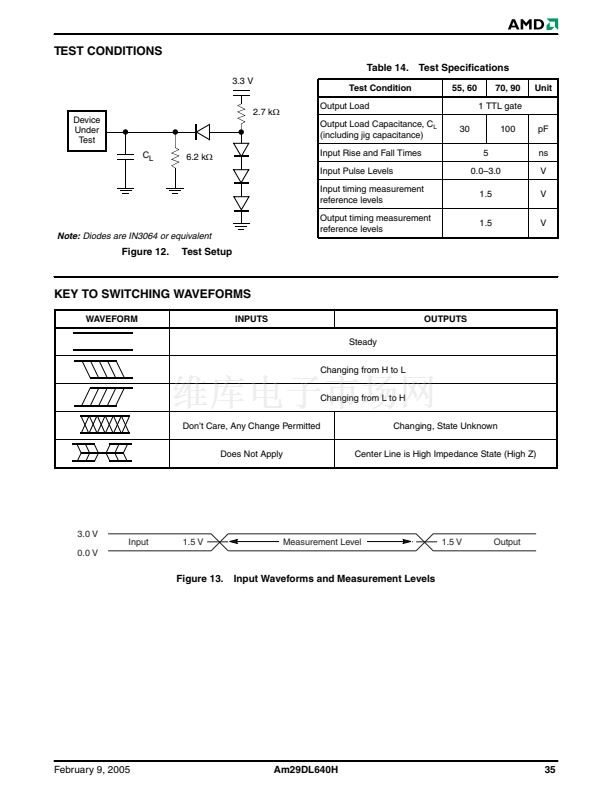
Test Conditions. . . . . . . . . . . . . . . . . . . . . . . . . . . 35
Figure 12. Test Setup.................................................................... 35
Figure 13. Input Waveforms and Measurement Levels ................. 35
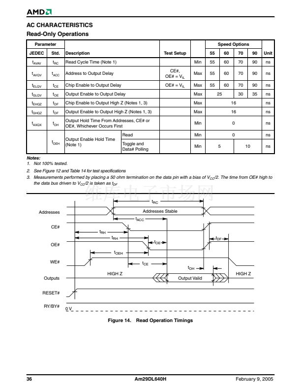
AC Characteristics . . . . . . . . . . . . . . . . . . . . . . . . 36
Read-Only Operations ........................................................... 36
Figure 14. Read Operation Timings ............................................... 36
Write Protect (WP#) ................................................................ 15
Table 7. WP#/ACC Modes ..............................................................16
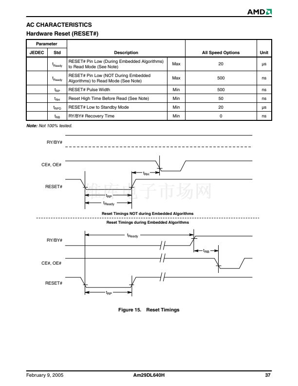
Hardware Reset (RESET#) .................................................... 37
Figure 15. Reset Timings ............................................................... 37
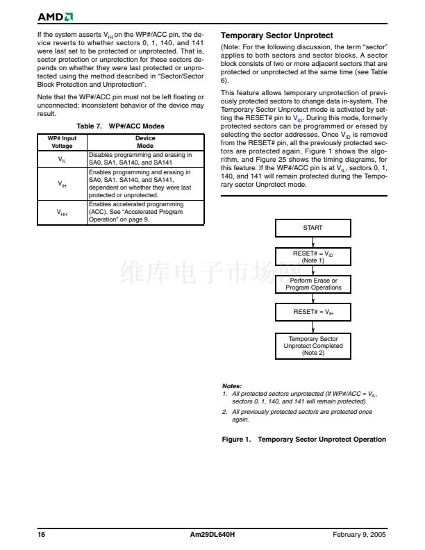
Temporary Sector Unprotect .................................................. 16
Figure 1. Temporary Sector Unprotect Operation........................... 16
Figure 2. In-System Sector Protect/Unprotect Algorithms .............. 17
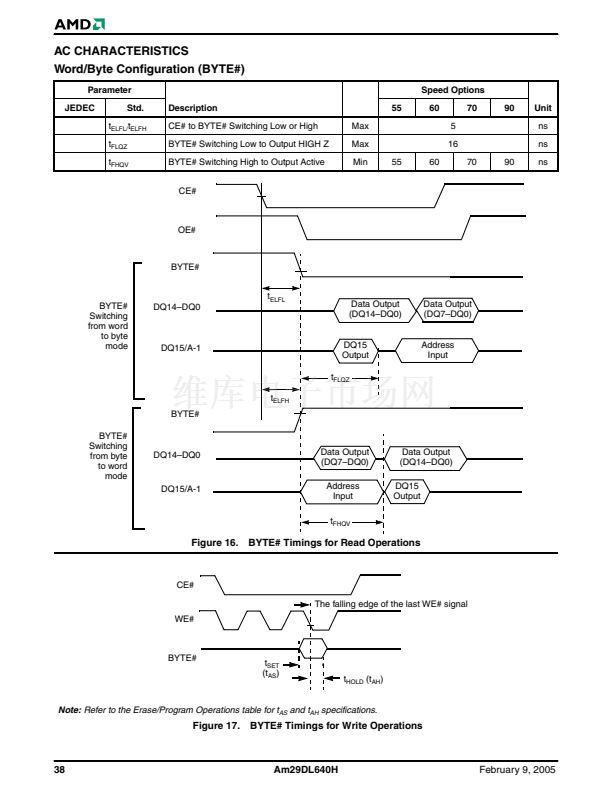
Word/Byte Configuration (BYTE#) .......................................... 38
Figure 16. BYTE# Timings for Read Operations............................ 38
Figure 17. BYTE# Timings for Write Operations............................ 38
Secured Silicon Sector
Flash Memory Region ............................................................ 18
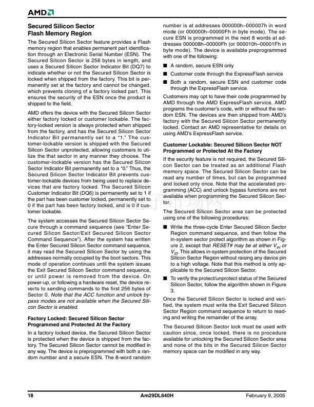
Figure 3. Secured Silicon Sector Protect Verify .............................. 19
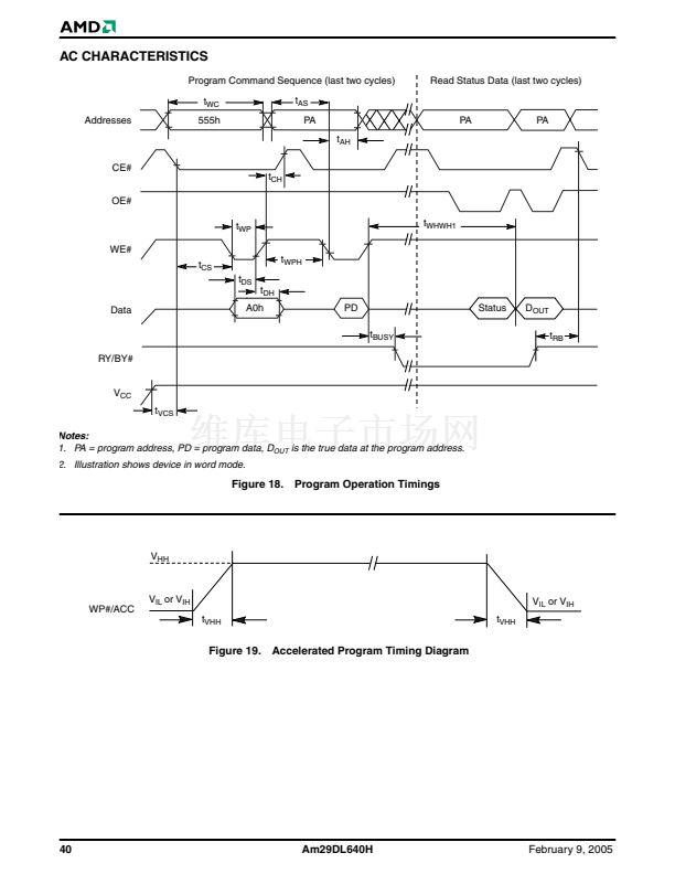
Erase and Program Operations .............................................. 39
Figure 18. Program Operation Timings..........................................
Figure 19. Accelerated Program Timing Diagram..........................
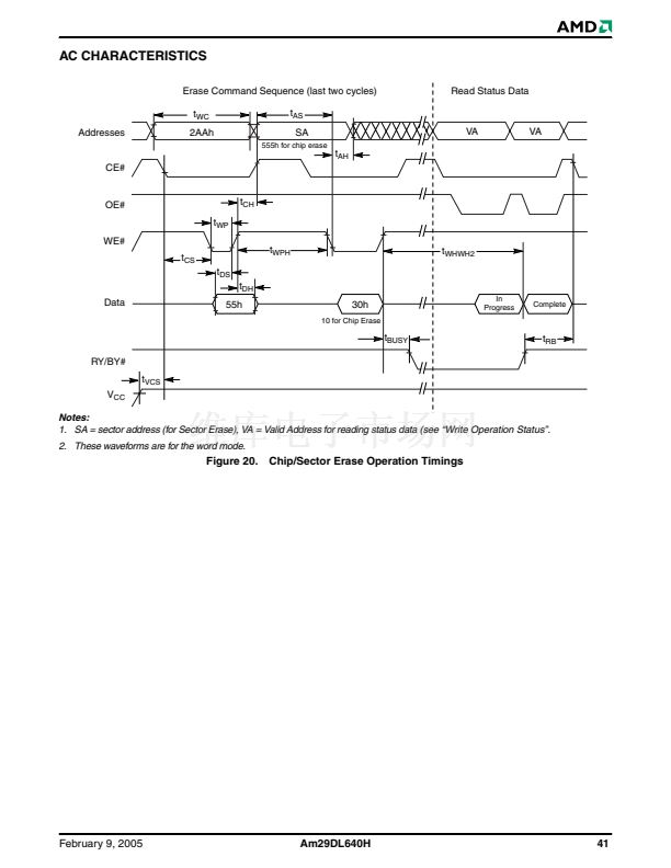
Figure 20. Chip/Sector Erase Operation Timings ..........................
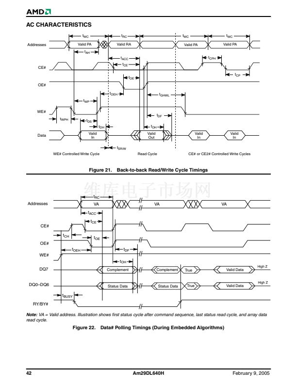
Figure 21. Back-to-back Read/Write Cycle Timings ......................
Figure 22. Data# Polling Timings (During Embedded Algorithms).
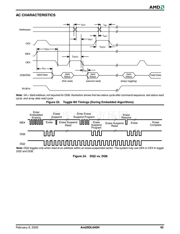
Figure 23. Toggle Bit Timings (During Embedded Algorithms)......
Figure 24. DQ2 vs. DQ6.................................................................
40
40
41
42
42
43
43
Hardware Data Protection ...................................................... 19
Low VCC Write Inhibit ............................................................ 19
Write Pulse 鈥淕litch鈥?Protection ............................................... 19
Logical Inhibit .......................................................................... 19
Power-Up Write Inhibit ............................................................ 19
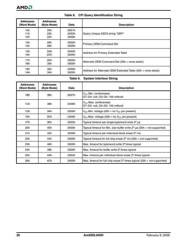
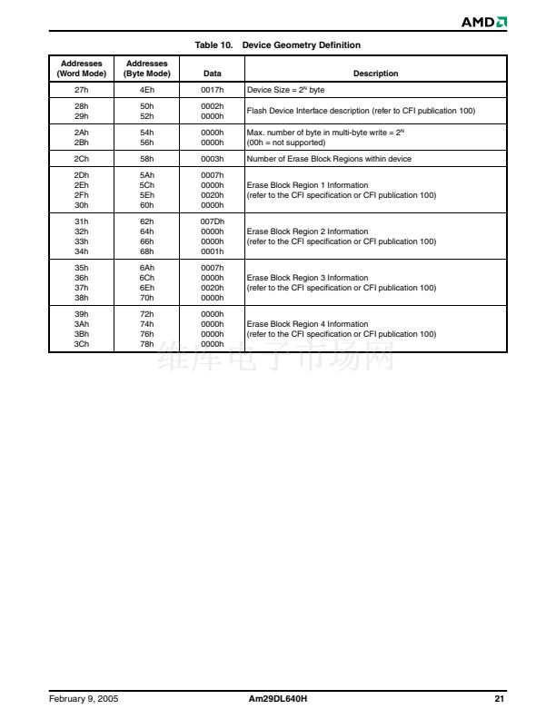
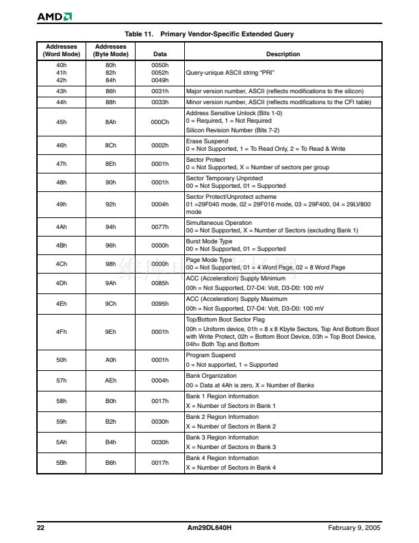
Common Flash Memory Interface (CFI) . . . . . . . 19
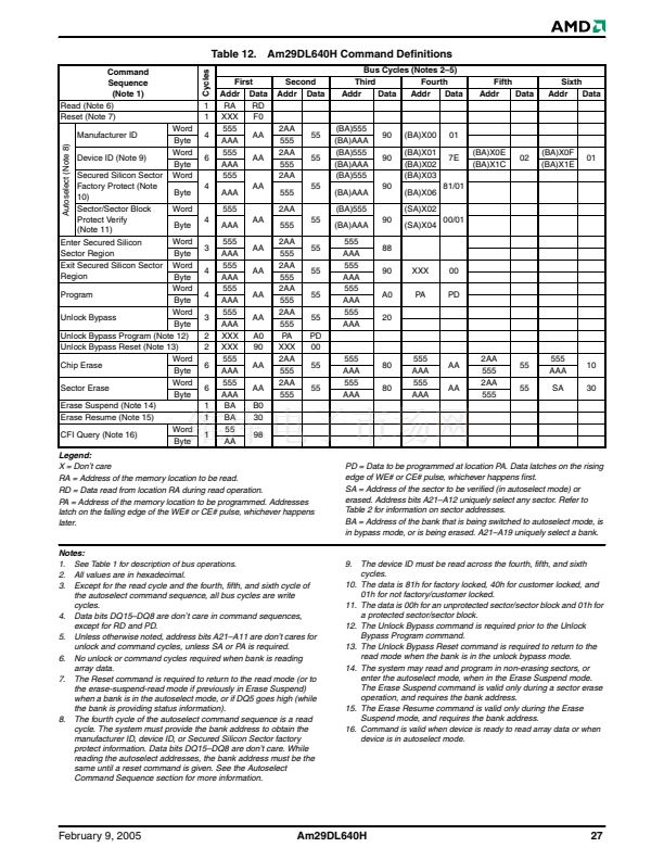
Command Definitions . . . . . . . . . . . . . . . . . . . . . 23
Reading Array Data ................................................................ 23
Reset Command ..................................................................... 23
Autoselect Command Sequence ............................................ 23
Enter Secured Silicon Sector/Exit Secured Silicon Sector
Command Sequence .............................................................. 23
Byte/Word Program Command Sequence ............................. 24
Unlock Bypass Command Sequence ..................................... 24
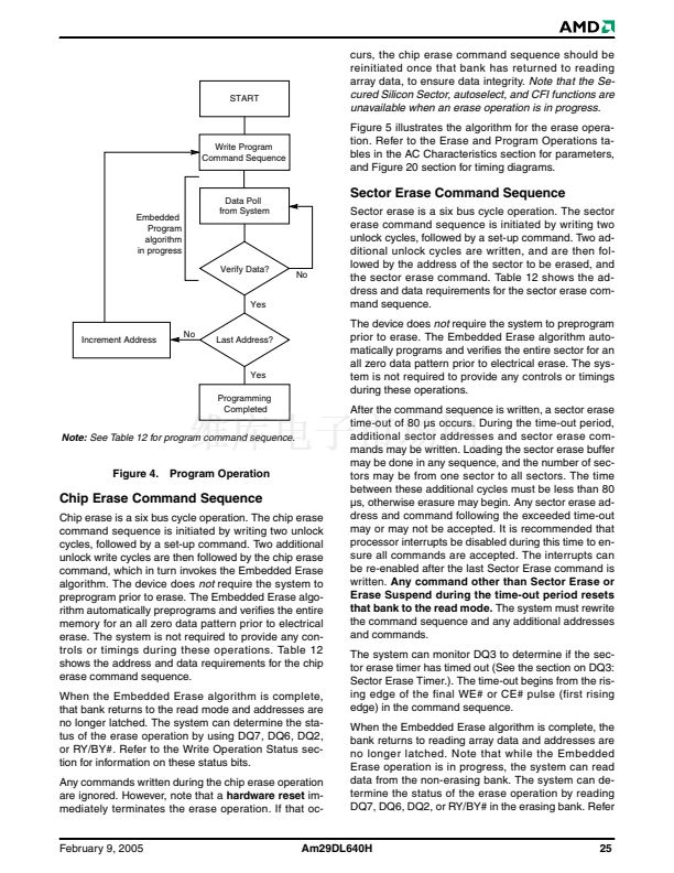
Figure 4. Program Operation .......................................................... 25
Temporary Sector Unprotect .................................................. 44
Figure 25. Temporary Sector Unprotect Timing Diagram .............. 44
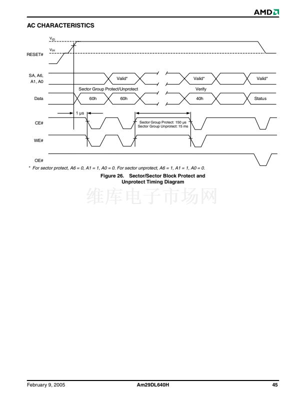
Figure 26. Sector/Sector Block Protect and
Unprotect Timing Diagram ............................................................. 45
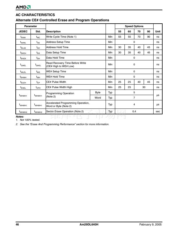
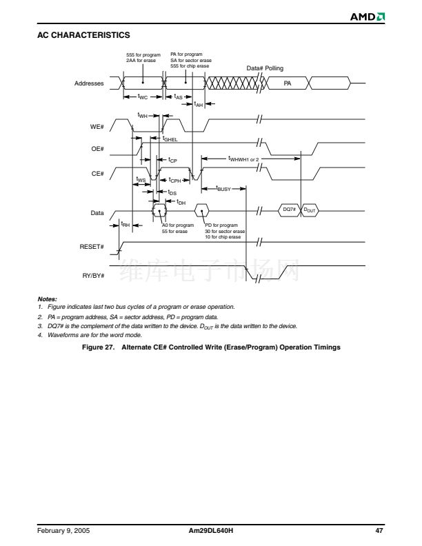
Alternate CE# Controlled Erase and Program Operations ..... 46
Figure 27. Alternate CE# Controlled Write (Erase/Program)
Operation Timings.......................................................................... 47
Chip Erase Command Sequence ........................................... 25
Sector Erase Command Sequence ........................................ 25
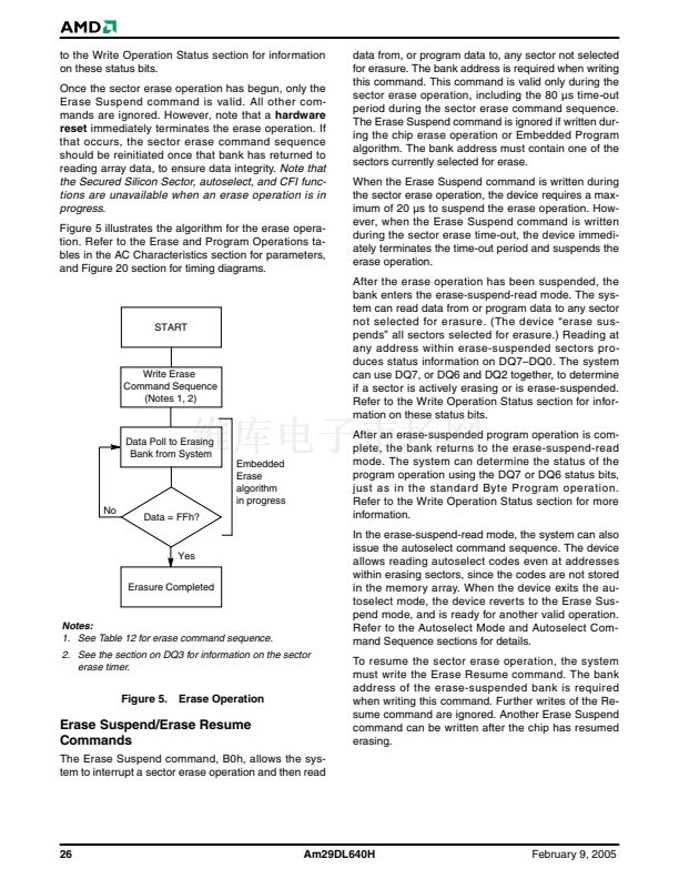
Figure 5. Erase Operation............................................................... 26
Erase Suspend/Erase Resume Commands ........................... 26
Write Operation Status . . . . . . . . . . . . . . . . . . . . 28
DQ7: Data# Polling ................................................................. 28
Figure 6. Data# Polling Algorithm ................................................... 28
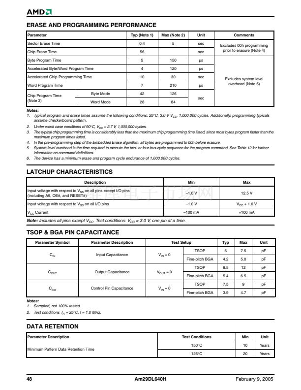
Erase And Programming Performance. . . . . . . . 48
Latchup Characteristics . . . . . . . . . . . . . . . . . . . . 48
TSOP & BGA Pin Capacitance. . . . . . . . . . . . . . . 48
Data Retention. . . . . . . . . . . . . . . . . . . . . . . . . . . . 48
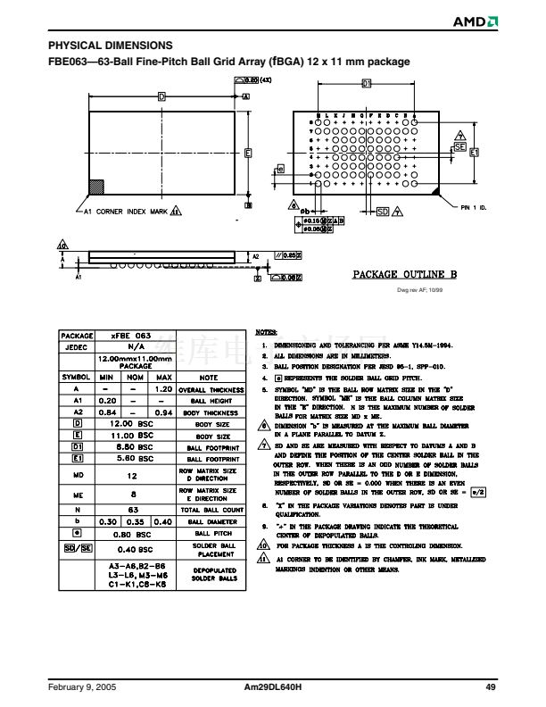
FBE063鈥?3-Ball Fine-Pitch Ball Grid Array (fBGA)
12 x 11 mm package .............................................................. 49
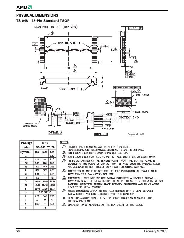
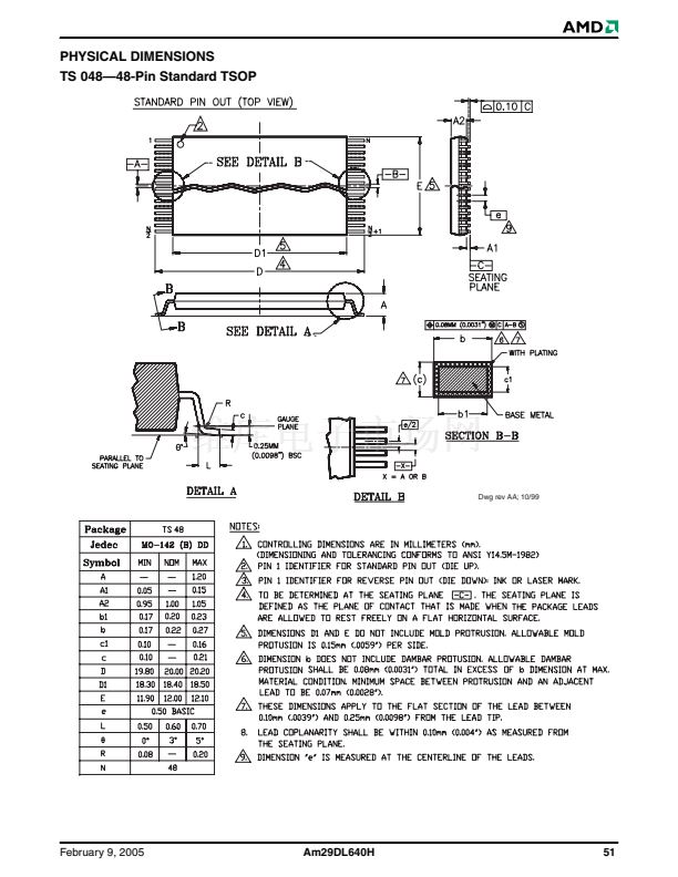
TS 048鈥?8-Pin Standard TSOP ............................................ 50
Physical Dimensions . . . . . . . . . . . . . . . . . . . . . . 51
TS 048鈥?8-Pin Standard TSOP. . . . . . . . . . . . . . 52
Revision Summary . . . . . . . . . . . . . . . . . . . . . . . . 53
February 9, 2005
Am29DL640H
3


 1
1
 2
2
 3
3
 4
4
 5
5
 6
6
 7
7
 8
8
 9
9
 10
10
 11
11
 12
12
 13
13
 14
14
 15
15
 16
16
 17
17
 18
18
 19
19
 20
20
 21
21
 22
22
 23
23
 24
24
 25
25
 26
26
 27
27
 28
28
 29
29
 30
30
 31
31
 32
32
 33
33
 34
34
 35
35
 36
36
 37
37
 38
38
 39
39
 40
40
 41
41
 42
42
 43
43
 44
44
 45
45
 46
46
 47
47
 48
48
 49
49
 50
50
 51
51
 52
52
 53
53
 54
54
