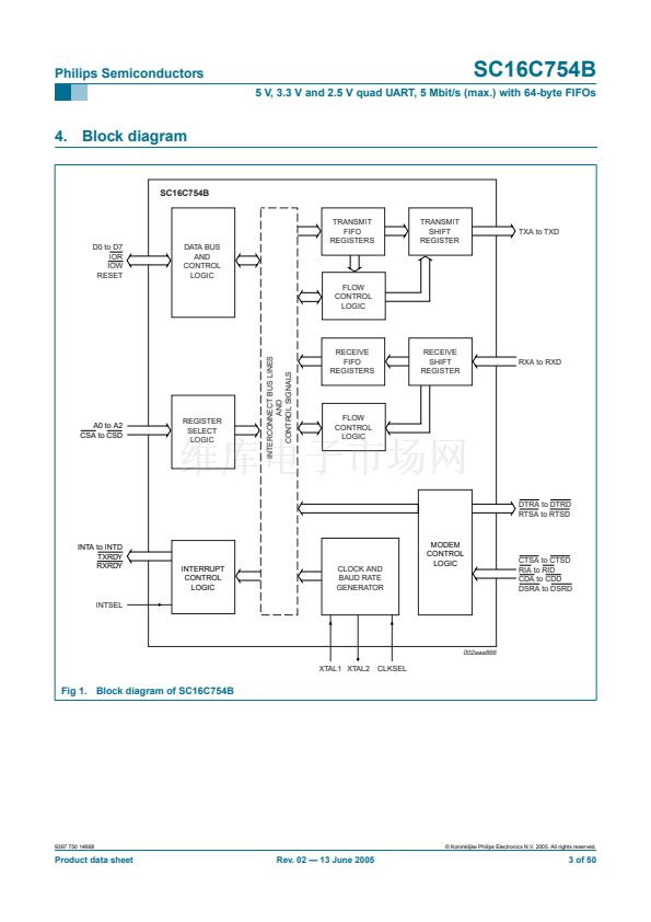
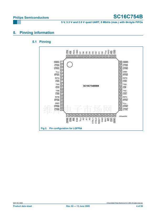
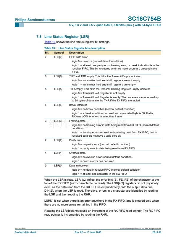
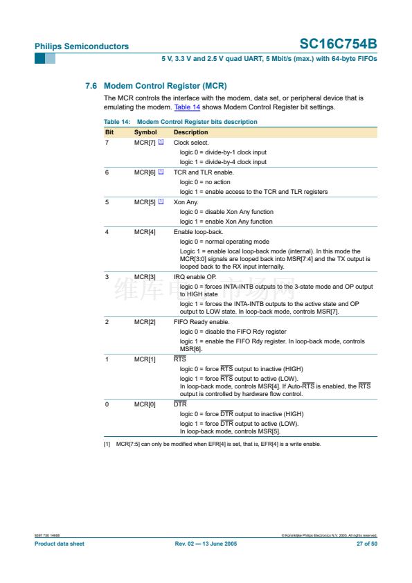
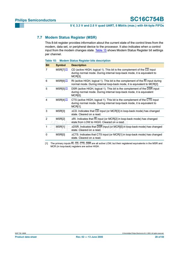
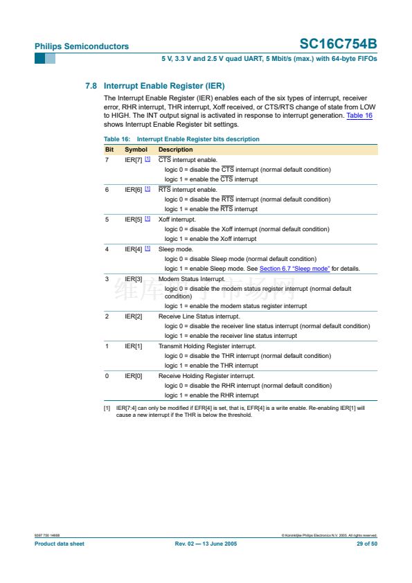
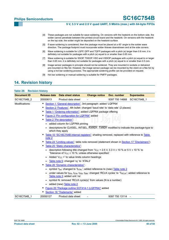
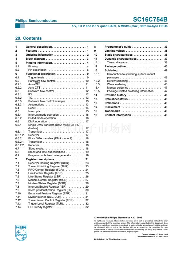
Philips Semiconductors
SC16C754B
5 V, 3.3 V and 2.5 V quad UART, 5 Mbit/s (max.) with 64-byte FIFOs
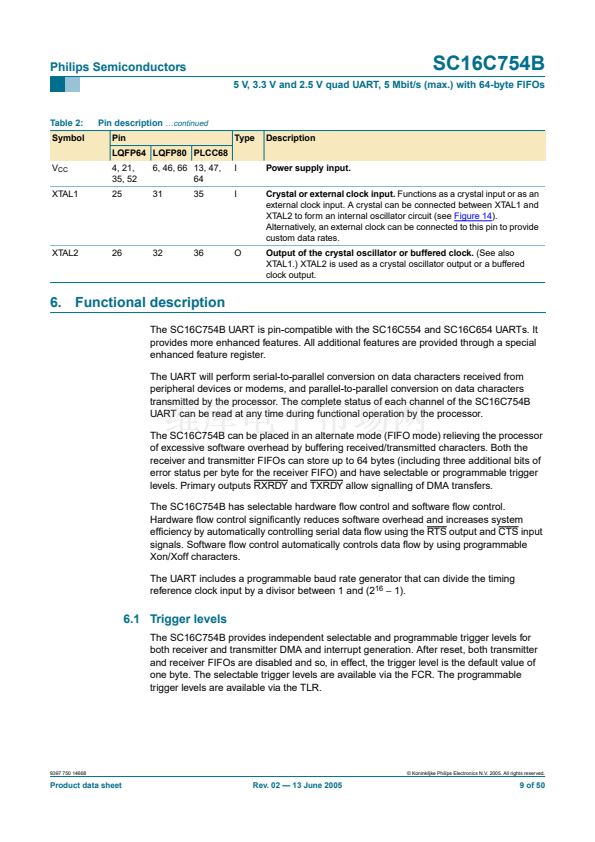
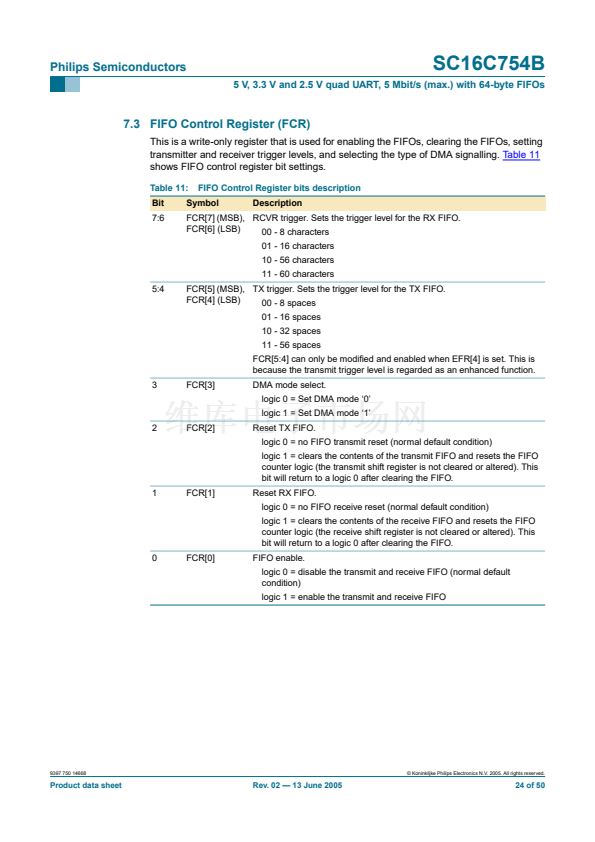
7.3 FIFO Control Register (FCR)
This is a write-only register that is used for enabling the FIFOs, clearing the FIFOs, setting
transmitter and receiver trigger levels, and selecting the type of DMA signalling.
Table 11
shows FIFO control register bit settings.
Table 11:
Bit
7:6
FIFO Control Register bits description
Description
Symbol
FCR[7] (MSB), RCVR trigger. Sets the trigger level for the RX FIFO.
FCR[6] (LSB)
00 - 8 characters
01 - 16 characters
10 - 56 characters
11 - 60 characters
5:4
FCR[5] (MSB), TX trigger. Sets the trigger level for the TX FIFO.
FCR[4] (LSB)
00 - 8 spaces
01 - 16 spaces
10 - 32 spaces
11 - 56 spaces
FCR[5:4] can only be modi铿乪d and enabled when EFR[4] is set. This is
because the transmit trigger level is regarded as an enhanced function.
3
FCR[3]
DMA mode select.
logic 0 = Set DMA mode 鈥?鈥?/div>
logic 1 = Set DMA mode 鈥?鈥?/div>
2
FCR[2]
Reset TX FIFO.
logic 0 = no FIFO transmit reset (normal default condition)
logic 1 = clears the contents of the transmit FIFO and resets the FIFO
counter logic (the transmit shift register is not cleared or altered). This
bit will return to a logic 0 after clearing the FIFO.
1
FCR[1]
Reset RX FIFO.
logic 0 = no FIFO receive reset (normal default condition)
logic 1 = clears the contents of the receive FIFO and resets the FIFO
counter logic (the receive shift register is not cleared or altered). This
bit will return to a logic 0 after clearing the FIFO.
0
FCR[0]
FIFO enable.
logic 0 = disable the transmit and receive FIFO (normal default
condition)
logic 1 = enable the transmit and receive FIFO
9397 750 14668
漏 Koninklijke Philips Electronics N.V. 2005. All rights reserved.
Product data sheet
Rev. 02 鈥?13 June 2005
24 of 50


 1
1
 2
2
 3
3
 4
4
 5
5
 6
6
 7
7
 8
8
 9
9
 10
10
 11
11
 12
12
 13
13
 14
14
 15
15
 16
16
 17
17
 18
18
 19
19
 20
20
 21
21
 22
22
 23
23
 24
24
 25
25
 26
26
 27
27
 28
28
 29
29
 30
30
 31
31
 32
32
 33
33
 34
34
 35
35
 36
36
 37
37
 38
38
 39
39
 40
40
 41
41
 42
42
 43
43
 44
44
 45
45
 46
46
 47
47
 48
48
 49
49
 50
50
