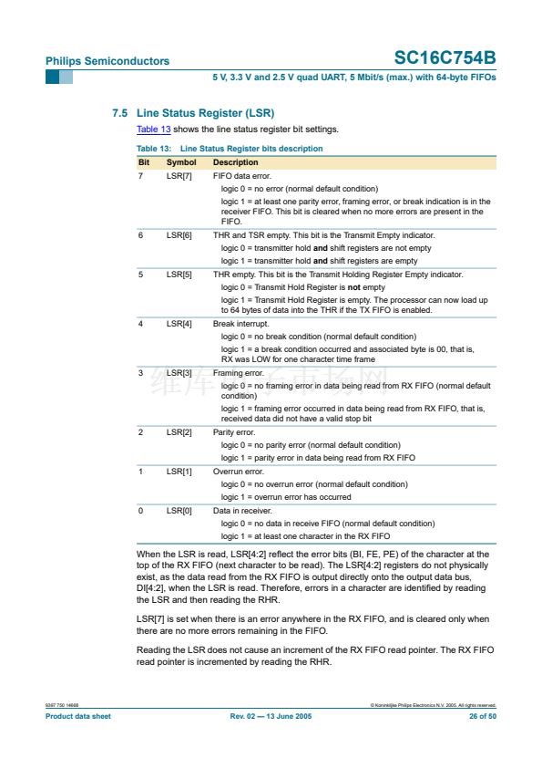
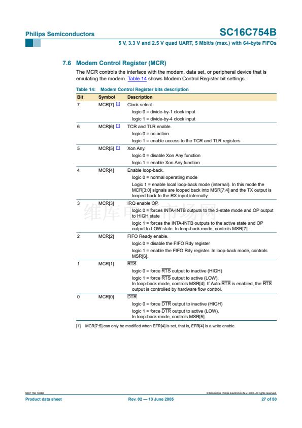
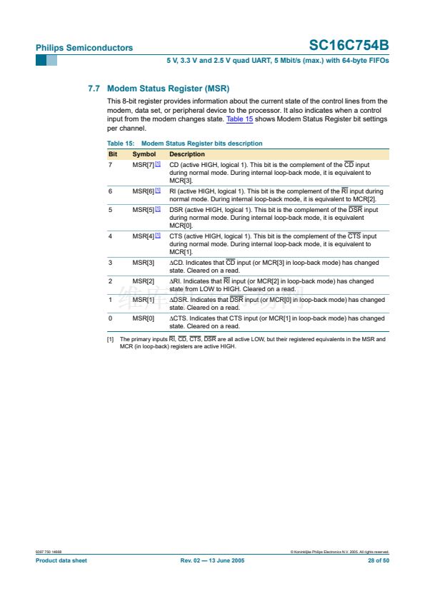
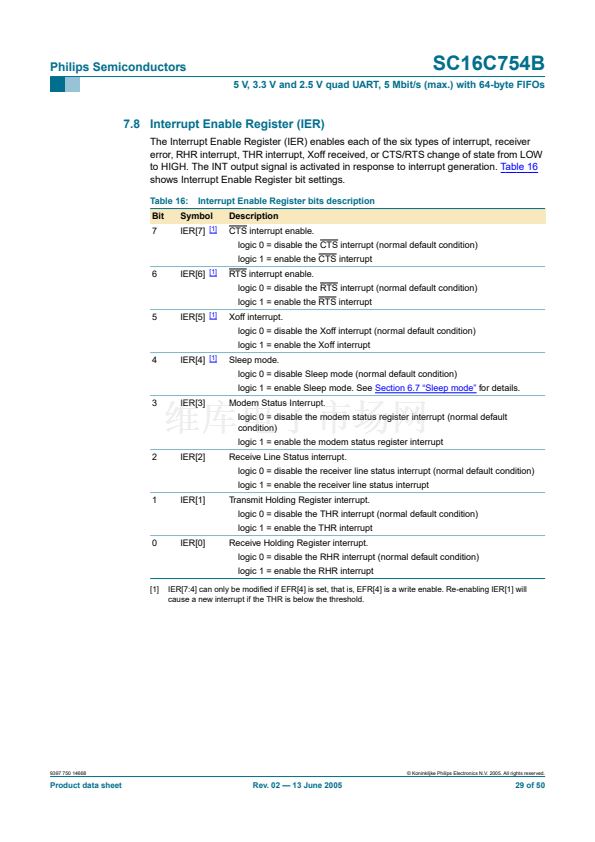
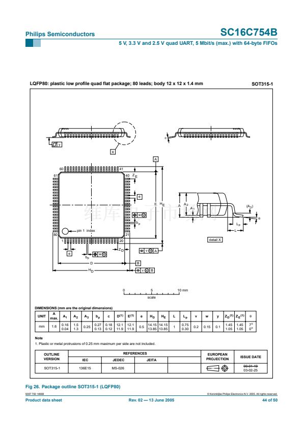
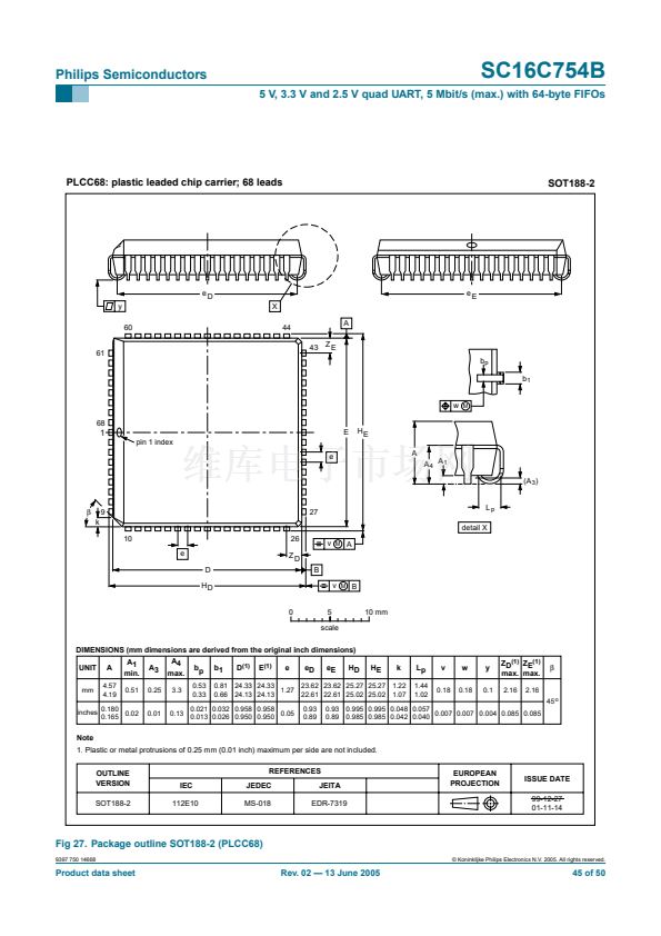
Philips Semiconductors
SC16C754B
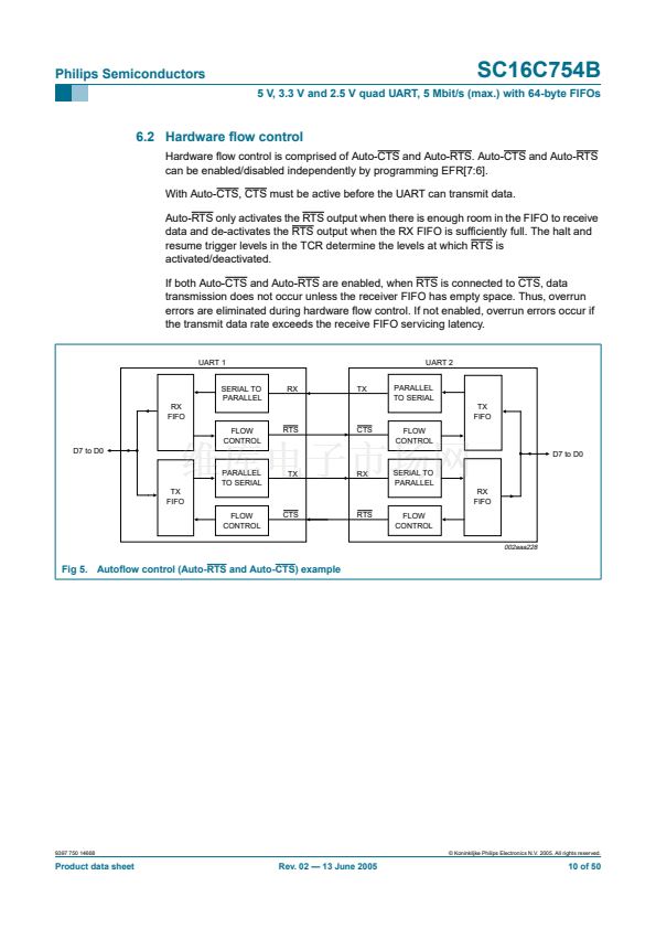
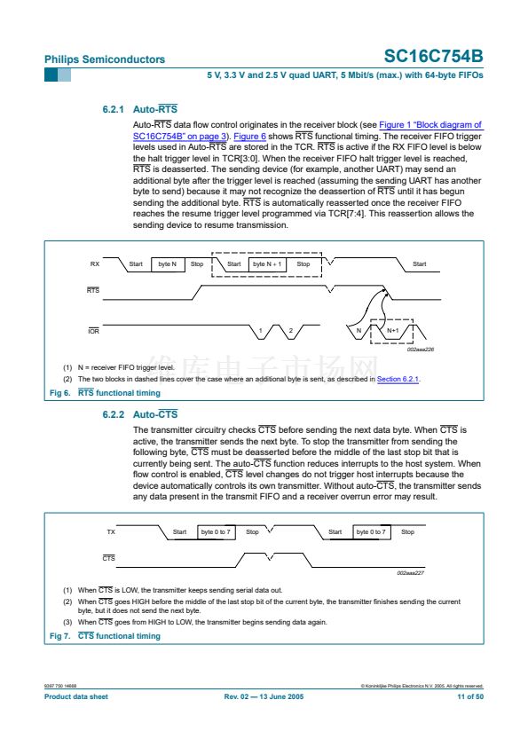
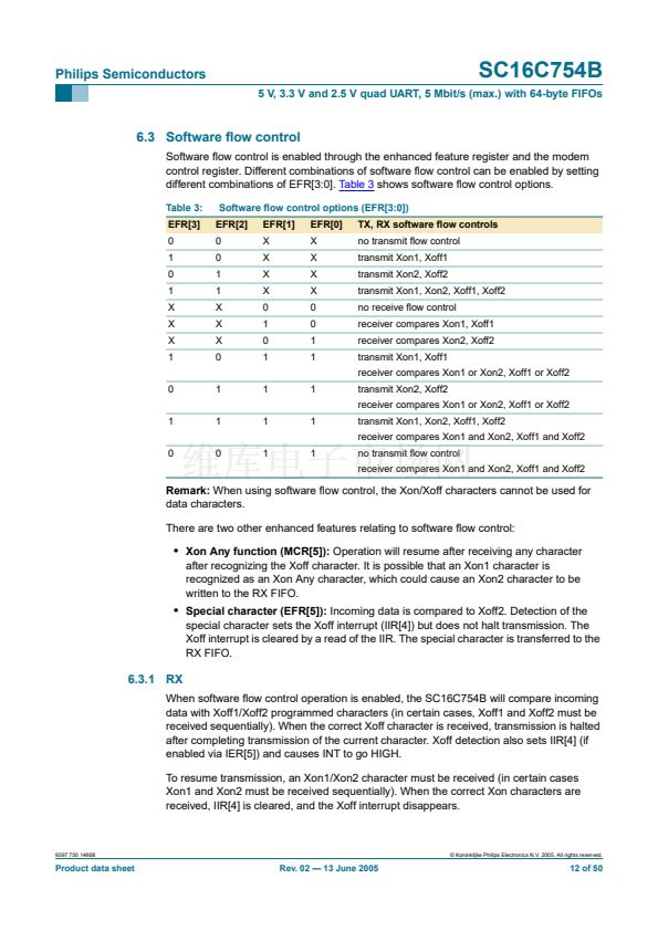
5 V, 3.3 V and 2.5 V quad UART, 5 Mbit/s (max.) with 64-byte FIFOs
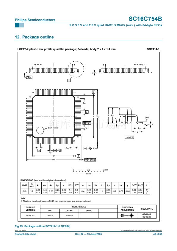
13. Soldering
13.1 Introduction to soldering surface mount packages
This text gives a very brief insight to a complex technology. A more in-depth account of
soldering ICs can be found in our
Data Handbook IC26; Integrated Circuit Packages
(document order number 9398 652 90011).
There is no soldering method that is ideal for all surface mount IC packages. Wave
soldering can still be used for certain surface mount ICs, but it is not suitable for 铿乶e pitch
SMDs. In these situations re铿俹w soldering is recommended.
13.2 Re铿俹w soldering
Re铿俹w soldering requires solder paste (a suspension of 铿乶e solder particles, 铿倁x and
binding agent) to be applied to the printed-circuit board by screen printing, stencilling or
pressure-syringe dispensing before package placement. Driven by legislation and
environmental forces the worldwide use of lead-free solder pastes is increasing.
Several methods exist for re铿俹wing; for example, convection or convection/infrared
heating in a conveyor type oven. Throughput times (preheating, soldering and cooling)
vary between 100 seconds and 200 seconds depending on heating method.
Typical re铿俹w peak temperatures range from 215
掳C
to 270
掳C
depending on solder paste
material. The top-surface temperature of the packages should preferably be kept:
鈥?/div>
below 225
掳C
(SnPb process) or below 245
掳C
(Pb-free process)
鈥?/div>
for all BGA, HTSSON..T and SSOP..T packages
鈥?/div>
for packages with a thickness
鈮?/div>
2.5 mm
鈥?/div>
for packages with a thickness < 2.5 mm and a volume
鈮?/div>
350 mm
3
so called
thick/large packages.
鈥?/div>
below 240
掳C
(SnPb process) or below 260
掳C
(Pb-free process) for packages with a
thickness < 2.5 mm and a volume < 350 mm
3
so called small/thin packages.
Moisture sensitivity precautions, as indicated on packing, must be respected at all times.
13.3 Wave soldering
Conventional single wave soldering is not recommended for surface mount devices
(SMDs) or printed-circuit boards with a high component density, as solder bridging and
non-wetting can present major problems.
To overcome these problems the double-wave soldering method was speci铿乧ally
developed.
If wave soldering is used the following conditions must be observed for optimal results:
鈥?/div>
Use a double-wave soldering method comprising a turbulent wave with high upward
pressure followed by a smooth laminar wave.
鈥?/div>
For packages with leads on two sides and a pitch (e):
鈥?/div>
larger than or equal to 1.27 mm, the footprint longitudinal axis is
preferred
to be
parallel to the transport direction of the printed-circuit board;
9397 750 14668
漏 Koninklijke Philips Electronics N.V. 2005. All rights reserved.
Product data sheet
Rev. 02 鈥?13 June 2005
46 of 50
SC16C754BIB80 产品属性
4
5Mbps
DMA 信号传输能力、软件可选择传输速率发生器
2.25V 到 5.5V
-40°C 到 +85°C
LQFP
80
No SVHC (18-Jun-2012)
异步
16
LQFP
-40°C
85°C
5Mbps
80MHz
5Mbps
5V
5V
2.5V
16C754
表??安装
16C754
SC16C754BIB80相关型号PDF文件下载
-
型号
版本
描述
厂商
下载
-
英文版
SC1602_ETC.pdf
ETC
-
英文版
THYRISTOR MODULE|TRIAC
ETC
-
英文版
THYRISTOR MODULE|TRIAC
ETC
-
英文版
THYRISTOR MODULE|TRIAC
ETC
-
英文版
THYRISTOR MODULE|TRIAC
ETC
-
英文版
THYRISTOR MODULE|TRIAC
ETC
-
英文版
THYRISTOR MODULE|TRIAC
ETC
-
英文版
HIGH-EFFICIENCY STEP-UP DC-DC CONVERTER
-
英文版
Semtech Corpora...
-
英文版
Semtech Corpora...
-
英文版
LOW VOLTAGE MULTI-MODE DC-DC CONVERTER
-
英文版
LOW VOLTAGE STEP-UP DC-DC CONVERTER
-
英文版
LOW VOLTAGE STEP-UP DC-DC CONVERTER
-
英文版
HIGH-VOLTAGE INVERTING DC-DC CONVERTER
-
英文版
MICROPOWER INVERTING DC-DC CONVERTER
-
英文版
THYRISTOR MODULE|TRIAC
ETC
-
英文版
THYRISTOR MODULE|TRIAC
ETC
-
英文版
THYRISTOR MODULE|TRIAC
ETC
-
英文版
THYRISTOR MODULE|TRIAC
ETC
-
英文版
THYRISTOR MODULE|TRIAC
ETC


 1
1
 2
2
 3
3
 4
4
 5
5
 6
6
 7
7
 8
8
 9
9
 10
10
 11
11
 12
12
 13
13
 14
14
 15
15
 16
16
 17
17
 18
18
 19
19
 20
20
 21
21
 22
22
 23
23
 24
24
 25
25
 26
26
 27
27
 28
28
 29
29
 30
30
 31
31
 32
32
 33
33
 34
34
 35
35
 36
36
 37
37
 38
38
 39
39
 40
40
 41
41
 42
42
 43
43
 44
44
 45
45
 46
46
 47
47
 48
48
 49
49
 50
50
