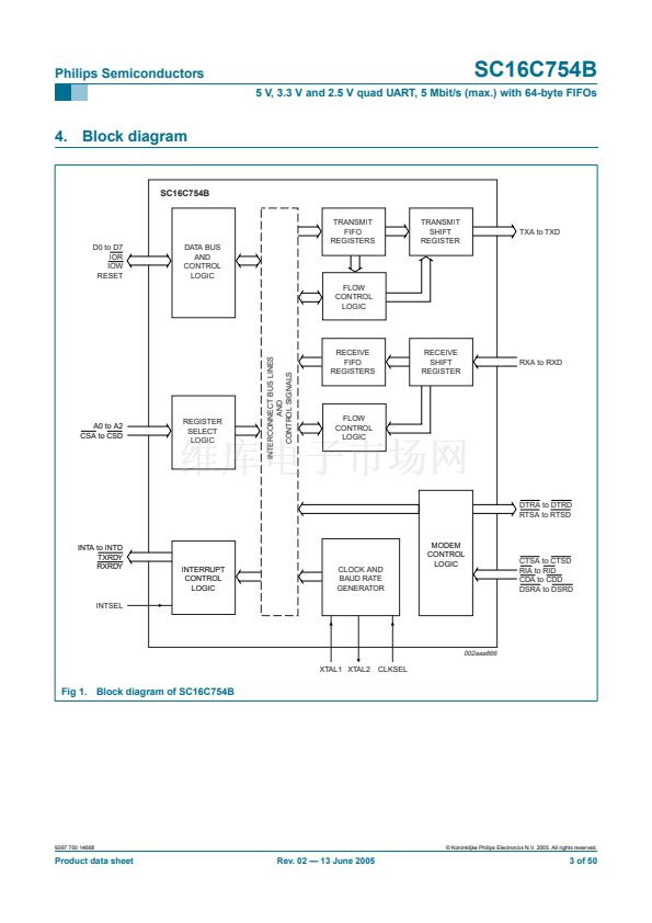
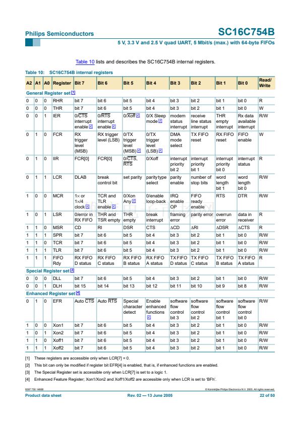
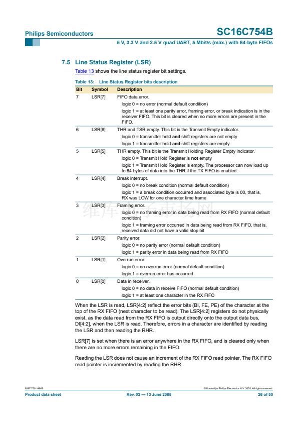
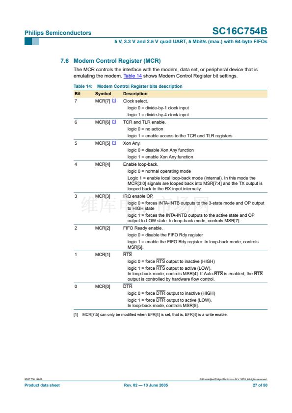
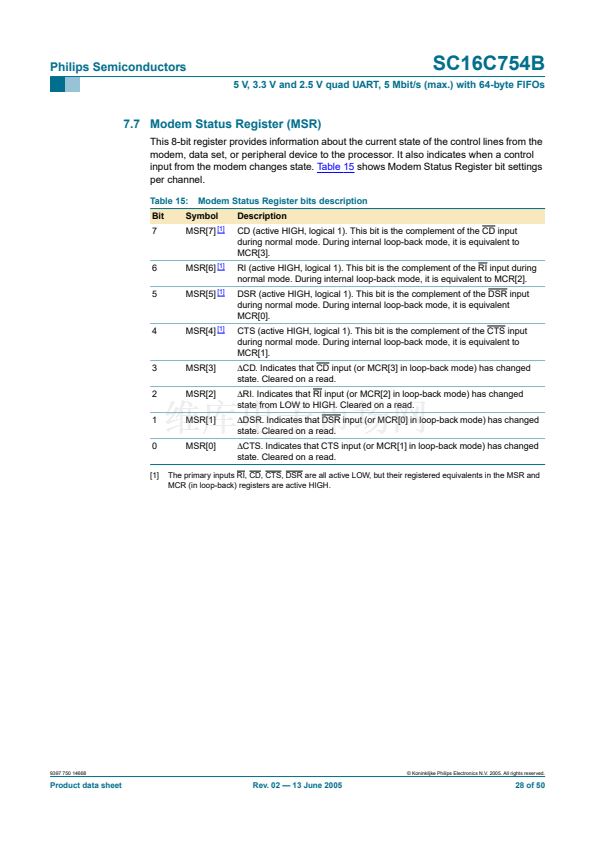
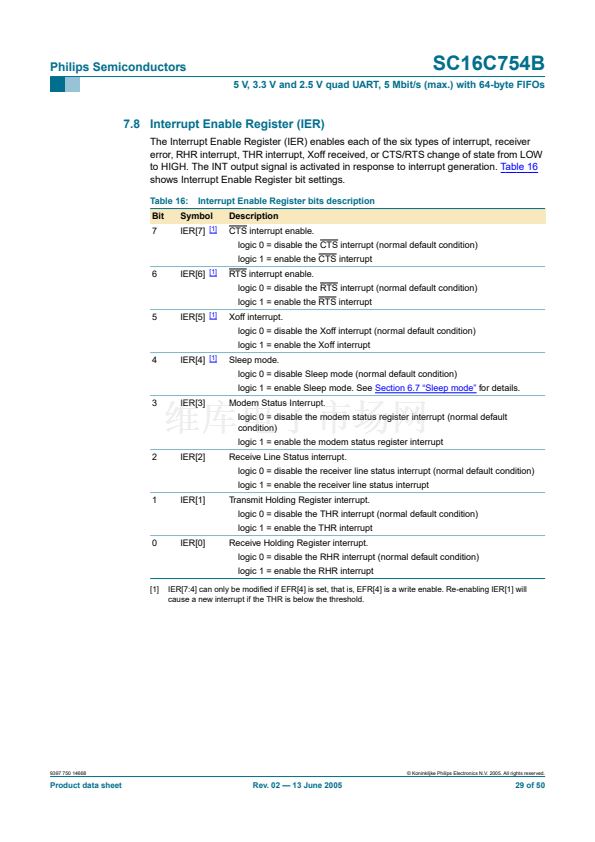
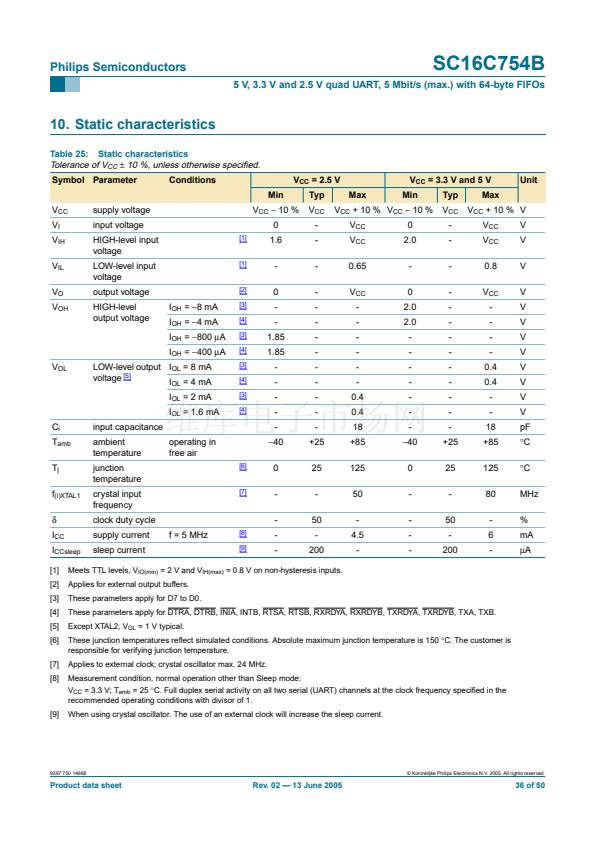
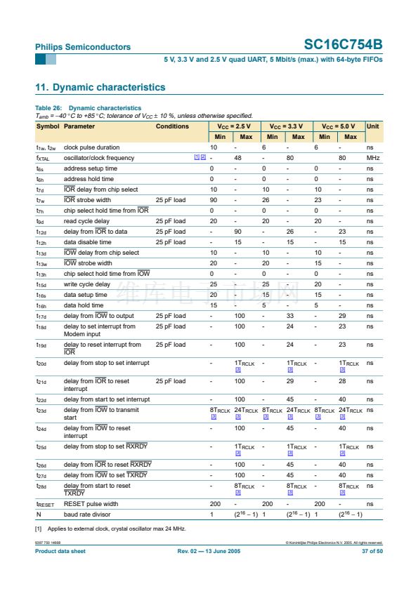
Philips Semiconductors
SC16C754B
5 V, 3.3 V and 2.5 V quad UART, 5 Mbit/s (max.) with 64-byte FIFOs
65 INTSEL
GND
DSRA 10
CTSA 11
DTRA 12
V
CC
13
RTSA 14
INTA 15
CSA 16
TXA 17
IOW 18
TXB 19
CSB 20
INTB 21
RTSB 22
GND 23
DTRB 24
CTSB 25
DSRB 26
CDB 27
RIB 28
RXB 29
CLKSEL 30
n.c. 31
A2 32
A1 33
A0 34
XTAL1 35
XTAL2 36
RESET 37
RXRDY 38
TXRDY 39
GND 40
RXC 41
RIC 42
CDC 43
61 CDD
60 DSRD
59 CTSD
58 DTRD
57 GND
56 RTSD
55 INTD
54 CSD
53 TXD
52 IOR
51 TXC
50 CSC
49 INTC
48 RTSC
47 V
CC
46 DTRC
45 CTSC
44 DSRC
002aaa868
CDA
63 RXD
RXA
64 V
CC
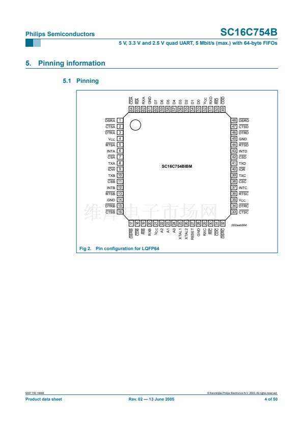
SC16C754BIA68
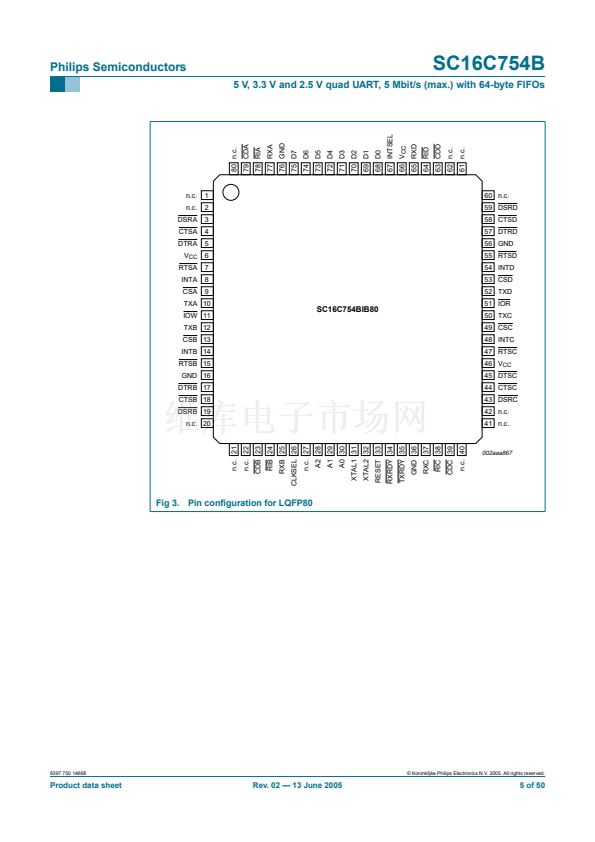
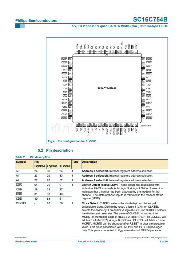
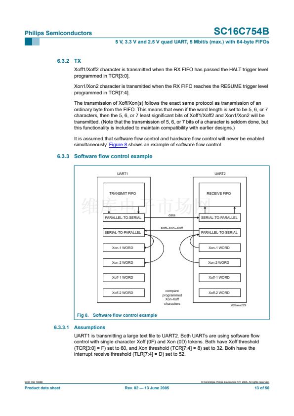
Fig 4. Pin con铿乬uration for PLCC68
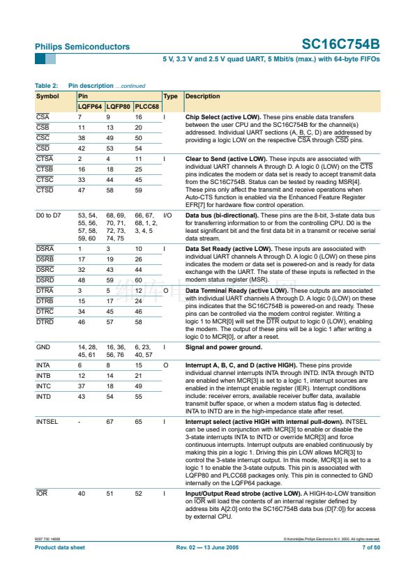
5.2 Pin description
Table 2:
Symbol
A0
A1
A2
CDA
CDB
CDC
CDD
CLKSEL
Pin description
Pin
LQFP64 LQFP80 PLCC68
24
23
22
64
18
31
49
-
30
29
28
79
23
39
63
26
34
33
32
9
27
43
61
30
I
I
I
I
I
Address 0 select bit.
Internal registers address selection.
Address 1 select bit.
Internal registers address selection.
Address 2 select bit.
Internal registers address selection.
Carrier Detect (active LOW).
These inputs are associated with
individual UART channels A through D. A logic LOW on these pins
indicates that a carrier has been detected by the modem for that
channel. The state of these inputs is re铿俥cted in the modem status
register (MSR).
Clock Select.
CLKSEL selects the divide-by-1 or divide-by-4
prescalable clock. During the reset, a logic 1 (V
CC
) on CLKSEL
selects the divide-by-1 prescaler. A logic 0 (GND) on CLKSEL selects
the divide-by-4 prescaler. The value of CLKSEL is latched into
MCR[7] at the trailing edge of RESET. A logic 1 (V
CC
) on CLKSEL will
latch a 0 into MCR[7]. A logic 0 (GND) on CLKSEL will latch a 1 into
MCR[7]. MCR[7] can be changed after RESET to alter the prescaler
value. This pin is associated with LQFP80 and PLCC68 packages
only. This pin is connected to V
CC
internally on LQFP64 package.
漏 Koninklijke Philips Electronics N.V. 2005. All rights reserved.
Type
Description
9397 750 14668
Product data sheet
Rev. 02 鈥?13 June 2005
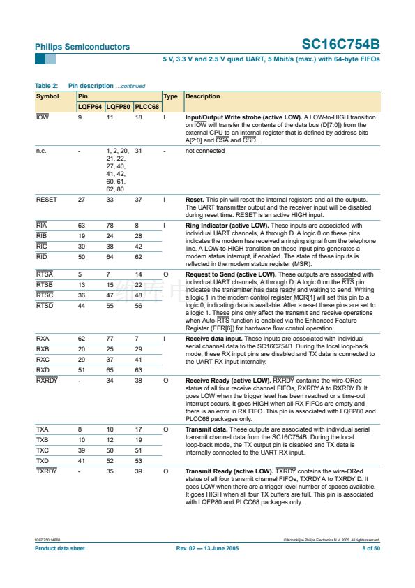
62 RID
RIA
D7
D6
D5
D4
D3
68 D2
67 D1
66 D0
9
8
7
6
5
4
3
2
1
6 of 50


 1
1
 2
2
 3
3
 4
4
 5
5
 6
6
 7
7
 8
8
 9
9
 10
10
 11
11
 12
12
 13
13
 14
14
 15
15
 16
16
 17
17
 18
18
 19
19
 20
20
 21
21
 22
22
 23
23
 24
24
 25
25
 26
26
 27
27
 28
28
 29
29
 30
30
 31
31
 32
32
 33
33
 34
34
 35
35
 36
36
 37
37
 38
38
 39
39
 40
40
 41
41
 42
42
 43
43
 44
44
 45
45
 46
46
 47
47
 48
48
 49
49
 50
50
