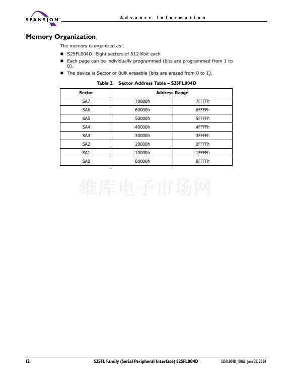
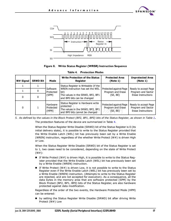
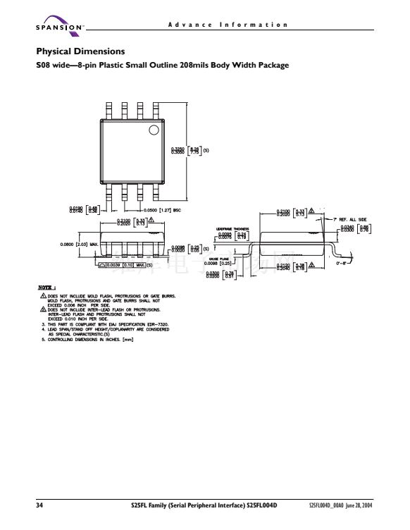
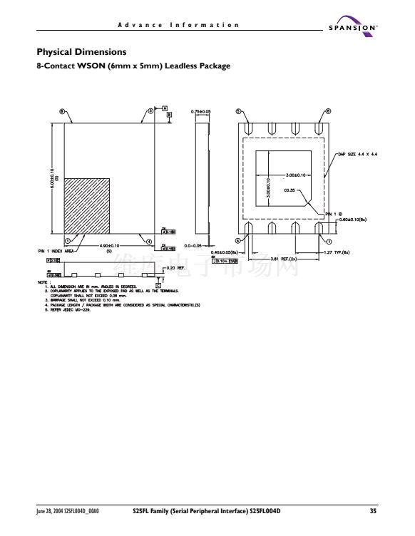
A d v a n c e
I n f o r m a t i o n
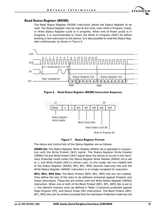
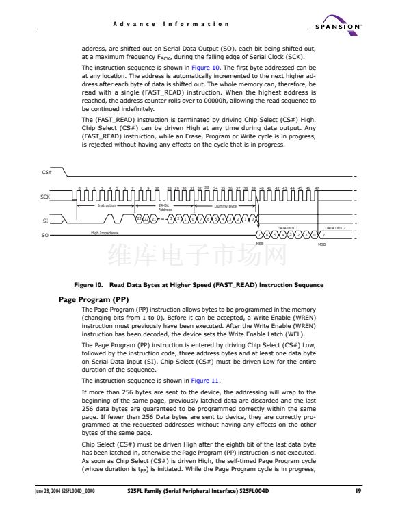
address, are shifted out on Serial Data Output (SO), each bit being shifted out,
at a maximum frequency F
SCK
, during the falling edge of Serial Clock (SCK).
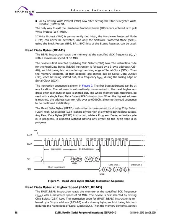
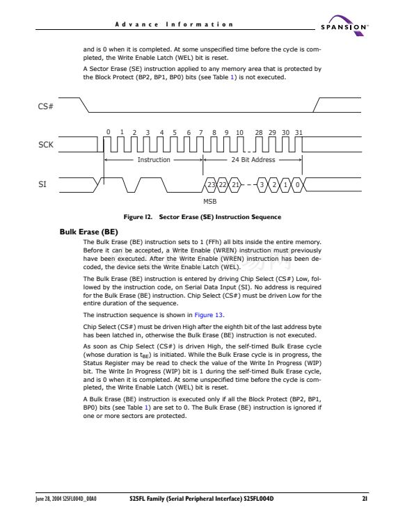
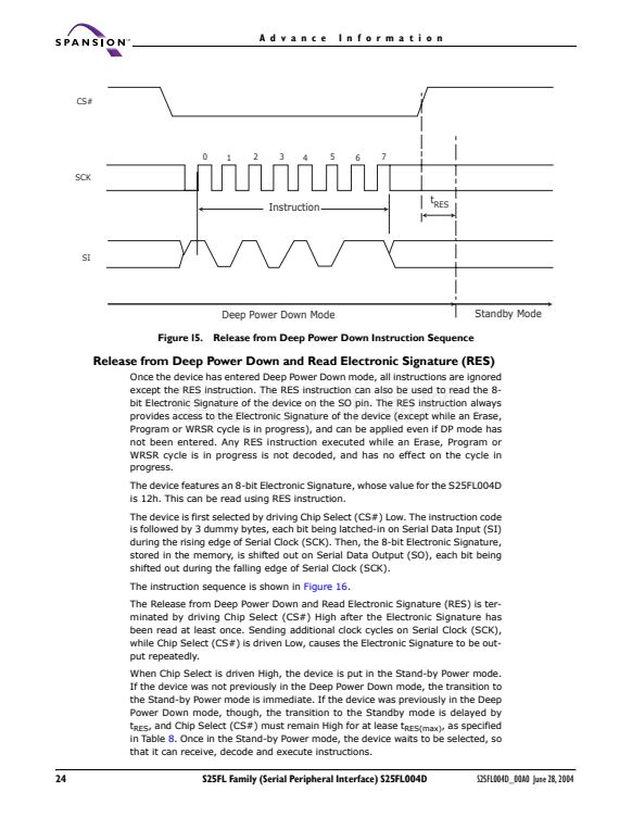
The instruction sequence is shown in
Figure 10.
The first byte addressed can be
at any location. The address is automatically incremented to the next higher ad-
dress after each byte of data is shifted out. The whole memory can, therefore, be
read with a single (FAST_READ) instruction. When the highest address is
reached, the address counter rolls over to 00000h, allowing the read sequence to
be continued indefinitely.
The (FAST_READ) instruction is terminated by driving Chip Select (CS#) High.
Chip Select (CS#) can be driven High at any time during data output. Any
(FAST_READ) instruction, while an Erase, Program or Write cycle is in progress,
is rejected without having any effects on the cycle that is in progress.
CS#
0
1
2
3
4
5
6
7
8
9
10
28 29 30
31 32 33
34 35 36 37 38
39
40 41
42 43 44 45
46
47
SCK
Instruction
23 22 21
24-Bit
Address
3
2
1
0
7
6
Dummy Byte
5
4
2
0
DATA OUT 1
DATA OUT 2
1
0
7
MSB
SI
SO
High Impedance
3
1
7
MSB
6
5
4
3
2
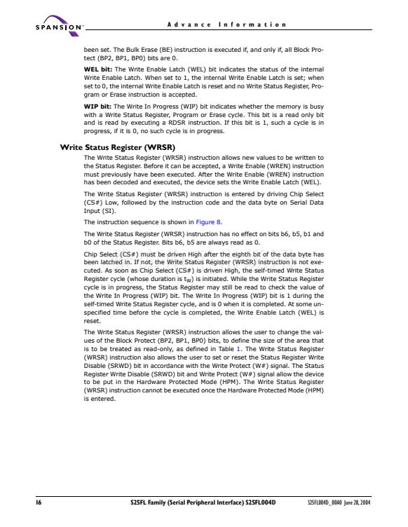
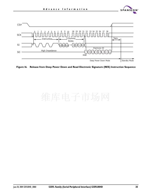
Figure 10.
Read Data Bytes at Higher Speed (FAST_READ) Instruction Sequence
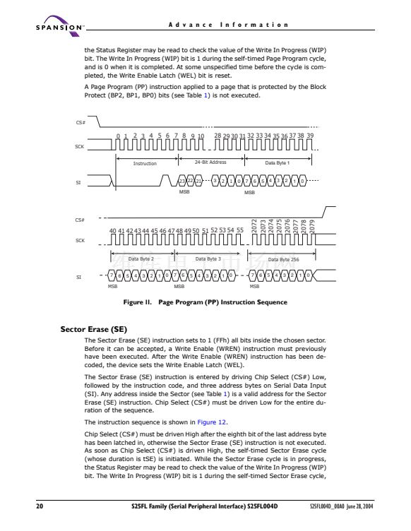
Page Program (PP)
The Page Program (PP) instruction allows bytes to be programmed in the memory
(changing bits from 1 to 0). Before it can be accepted, a Write Enable (WREN)
instruction must previously have been executed. After the Write Enable (WREN)
instruction has been decoded, the device sets the Write Enable Latch (WEL).
The Page Program (PP) instruction is entered by driving Chip Select (CS#) Low,
followed by the instruction code, three address bytes and at least one data byte
on Serial Data Input (SI). Chip Select (CS#) must be driven Low for the entire
duration of the sequence.
The instruction sequence is shown in
Figure 11.
If more than 256 bytes are sent to the device, the addressing will wrap to the
beginning of the same page, previously latched data are discarded and the last
256 data bytes are guaranteed to be programmed correctly within the same
page. If fewer than 256 Data bytes are sent to device, they are correctly pro-
grammed at the requested addresses without having any effects on the other
bytes of the same page.
Chip Select (CS#) must be driven High after the eighth bit of the last data byte
has been latched in, otherwise the Page Program (PP) instruction is not executed.
As soon as Chip Select (CS#) is driven High, the self-timed Page Program cycle
(whose duration is t
PP
) is initiated. While the Page Program cycle is in progress,
June 28, 2004 S25FL004D_00A0
S25FL Family (Serial Peripheral Interface) S25FL004D
19


 1
1
 2
2
 3
3
 4
4
 5
5
 6
6
 7
7
 8
8
 9
9
 10
10
 11
11
 12
12
 13
13
 14
14
 15
15
 16
16
 17
17
 18
18
 19
19
 20
20
 21
21
 22
22
 23
23
 24
24
 25
25
 26
26
 27
27
 28
28
 29
29
 30
30
 31
31
 32
32
 33
33
 34
34
 35
35
 36
36
