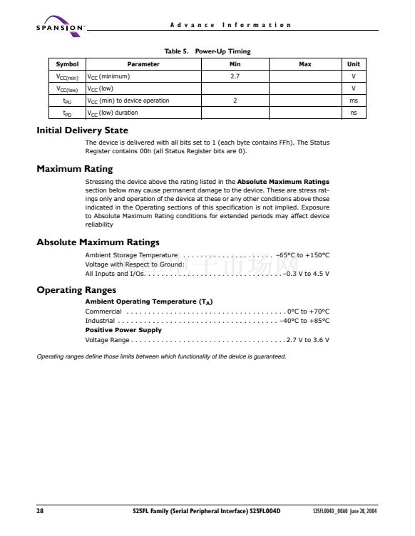
A d v a n c e
I n f o r m a t i o n
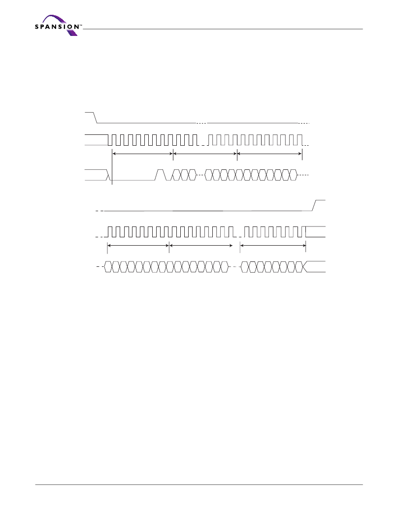
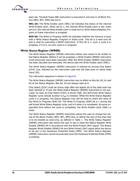
the Status Register may be read to check the value of the Write In Progress (WIP)
bit. The Write In Progress (WIP) bit is 1 during the self-timed Page Program cycle,
and is 0 when it is completed. At some unspecified time before the cycle is com-
pleted, the Write Enable Latch (WEL) bit is reset.
A Page Program (PP) instruction applied to a page that is protected by the Block
Protect (BP2, BP1, BP0) bits (see Table
1)
is not executed.
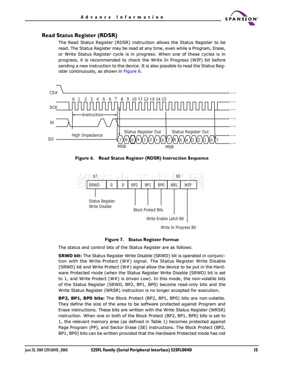
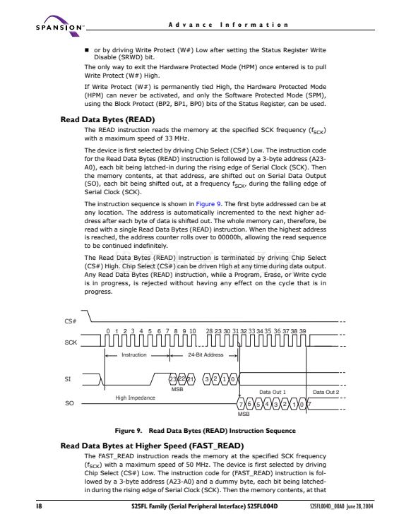
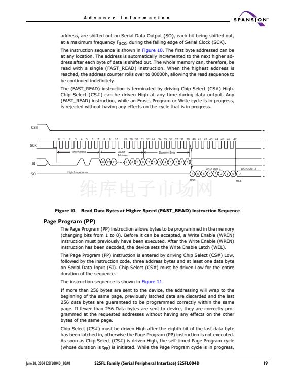
CS#
0 1 2 3 4 5 6 7 8 9 10
SCK
28 29 30 31 32 33 34 35 36 37 38 39
Instruction
24-Bit Address
Data Byte 1
SI
23 22 21
MSB
3
2
1
0
7
6
5
4
3
2
1
0
MSB
2072
7
MSB
40 41 42 43 44 45 46 47 48 49 50 51 52 53 54 55
SCK
Data Byte 2
Data Byte 3
SI
7
MSB
6
5
4
3
2
1
0
7
6
5
4
3
2
1
0
6
MSB
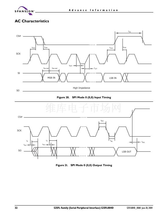
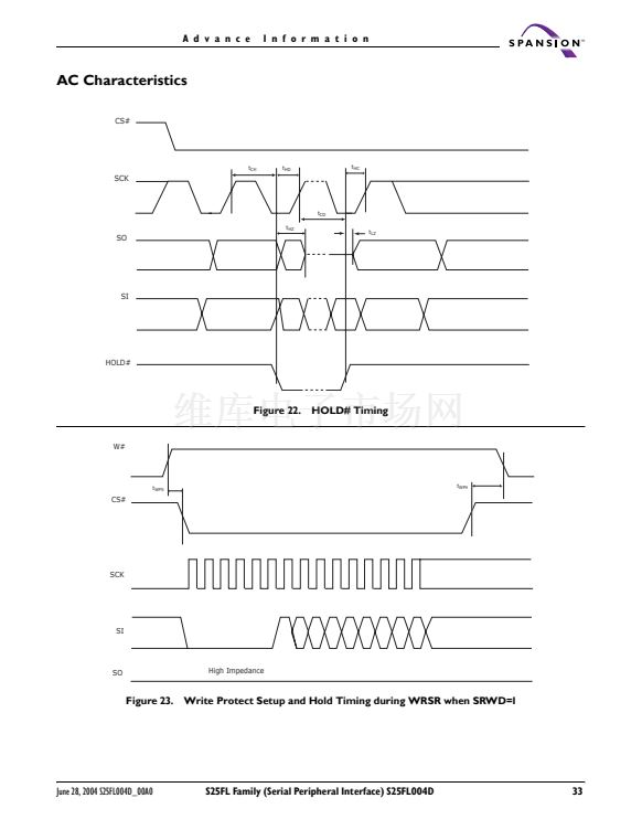
Figure 11.
Page Program (PP) Instruction Sequence
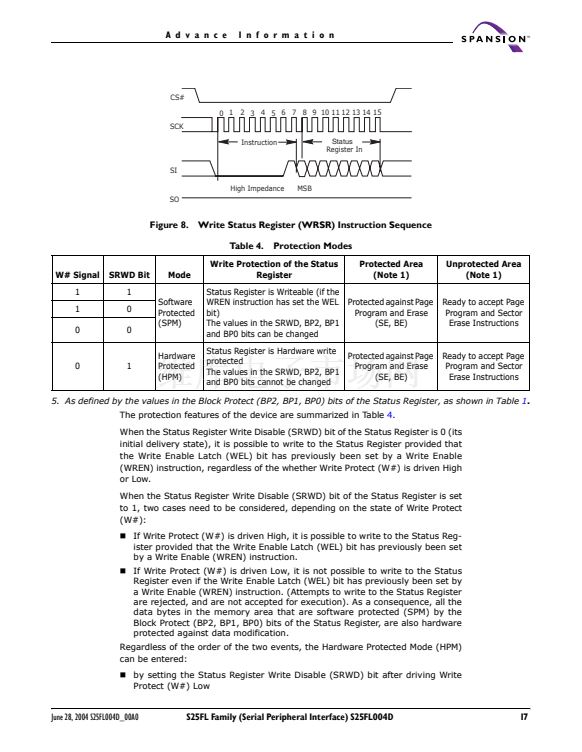
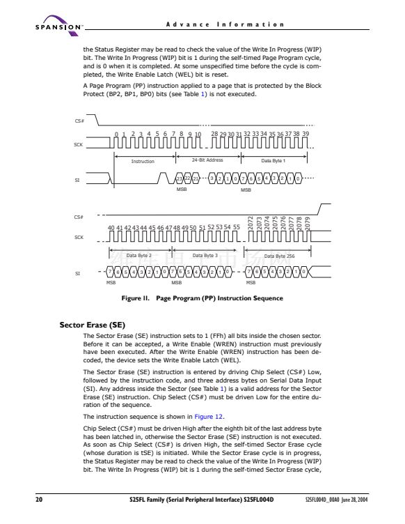
Sector Erase (SE)
The Sector Erase (SE) instruction sets to 1 (FFh) all bits inside the chosen sector.
Before it can be accepted, a Write Enable (WREN) instruction must previously
have been executed. After the Write Enable (WREN) instruction has been de-
coded, the device sets the Write Enable Latch (WEL).
The Sector Erase (SE) instruction is entered by driving Chip Select (CS#) Low,
followed by the instruction code, and three address bytes on Serial Data Input
(SI). Any address inside the Sector (see Table
1)
is a valid address for the Sector
Erase (SE) instruction. Chip Select (CS#) must be driven Low for the entire du-
ration of the sequence.
The instruction sequence is shown in
Figure 12.
Chip Select (CS#) must be driven High after the eighth bit of the last address byte
has been latched in, otherwise the Sector Erase (SE) instruction is not executed.
As soon as Chip Select (CS#) is driven High, the self-timed Sector Erase cycle
(whose duration is tSE) is initiated. While the Sector Erase cycle is in progress,
the Status Register may be read to check the value of the Write In Progress (WIP)
bit. The Write In Progress (WIP) bit is 1 during the self-timed Sector Erase cycle,
20
S25FL Family (Serial Peripheral Interface) S25FL004D
2073
2074
2075
2076
2077
2078
2079
Data Byte 256
5
4
3
2
1
0
CS#
S25FL004D_00A0 June 28, 2004


 1
1
 2
2
 3
3
 4
4
 5
5
 6
6
 7
7
 8
8
 9
9
 10
10
 11
11
 12
12
 13
13
 14
14
 15
15
 16
16
 17
17
 18
18
 19
19
 20
20
 21
21
 22
22
 23
23
 24
24
 25
25
 26
26
 27
27
 28
28
 29
29
 30
30
 31
31
 32
32
 33
33
 34
34
 35
35
 36
36
