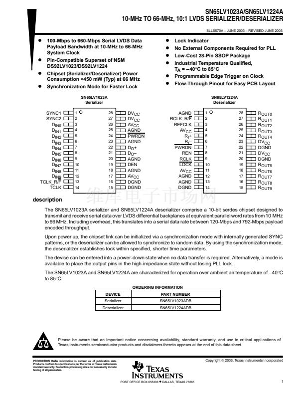
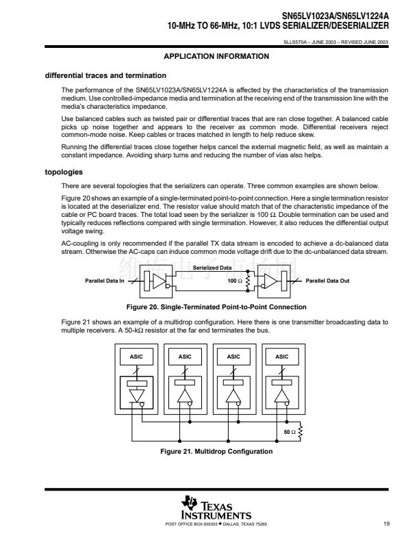
SN65LV1023A/SN65LV1224A
10-MHz TO 66-MHz, 10:1 LVDS SERIALIZER/DESERIALIZER
SLLS570A 鈥?JUNE 2003 鈥?REVISED JUNE 2003
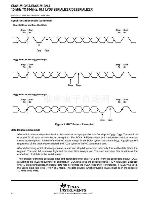
serializer timing requirements for TCLK over recommended operating supply and temperature
ranges (unless otherwise specified)
PARAMETER
tTCP
tTCIH
tTCIL
tt(CLK)
tJIT
Transmit clock period
Transmit clock high time
Transmit clock low time
TCLK input transition time
TCLK input jitter
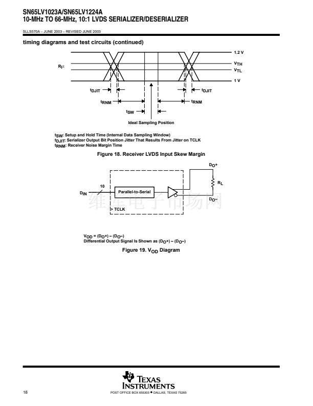
See Figure 18
TEST CONDITIONS
MIN
15.15
0.4T
0.4T
TYP
T
0.5T
0.5T
3
MAX
100
0.6T
0.6T
6
150
UNIT
ns
ns
ns
ns
ps
(RMS)
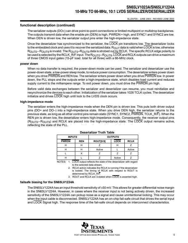
serializer switching characteristics over recommended operating supply and temperature ranges
(unless otherwise specified)
PARAMETER
tTLH(L)
tLTHL(L)
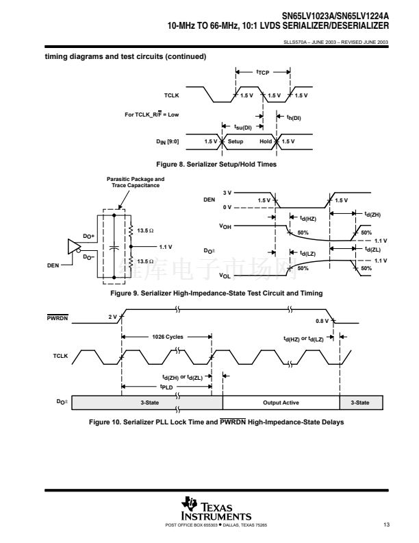
tsu(DI)
tsu(DI)
td(HZ)
td(LZ)
td(ZH)
td(ZL)
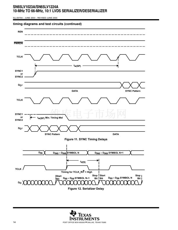
tw(SPW)
t(PLD)
td(S)
tDJIT
tRJIT
LVDS low-to-high transition time
LVDS high-to-low transition time
DIN0鈥揇IN9 setup to TCLK
DIN0鈥揇IN9 hold from TCLK
DO卤 high-to-high-impedance-state delay
DO卤 low-to-high-impedance-state delay
DO卤 high-to-high-impedance-state-to-
high delay
DO卤 high-to-high-impedance-state-to-low
delay
SYNC pulse duration
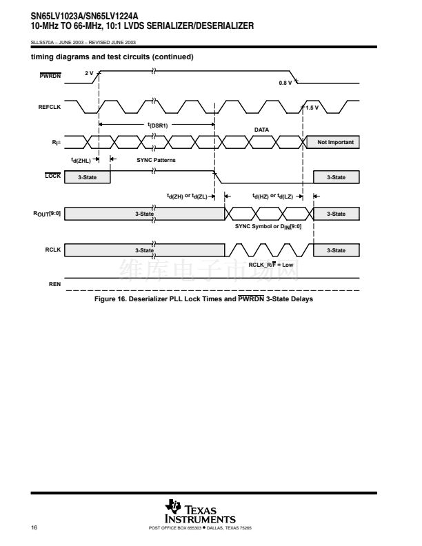
Serializer PLL lock time
Serializer delay
10 MHz
Deterministic jitter
Random jitter
66 MHz
RL = 27
鈩?/div>
See Figure 11
鈩?
RL = 27
鈩?
See Figure 12
RL = 27
鈩?/div>
CL = 10 pF to GND
鈩?
RL = 2.7
鈩?
CL = 10 pF to GND
10
6脳tTCP
1026脳tTCP
tTCP+1
tTCP+2
tTCP+3
230
150
19
RL = 27
鈩?
CL = 10 pF to GND,
See Figure 9
TEST CONDITIONS
RL = 27
鈩?
CL = 10 pF to GND,
F
See Figure 5
RL = 27
鈩?
CL = 10 pF to GND,
F
See Figure 8
0.5
4
2.5
2.5
5
6.5
5
5
10
10
ns
ns
ns
ps
ps
(RMS)
ns
MIN
TYP
0.2
0.25
MAX
0.4
0.4
UNIT
ns
ns
ns
ns
POST OFFICE BOX 655303
鈥?/div>
DALLAS, TEXAS 75265
9


 1
1
 2
2
 3
3
 4
4
 5
5
 6
6
 7
7
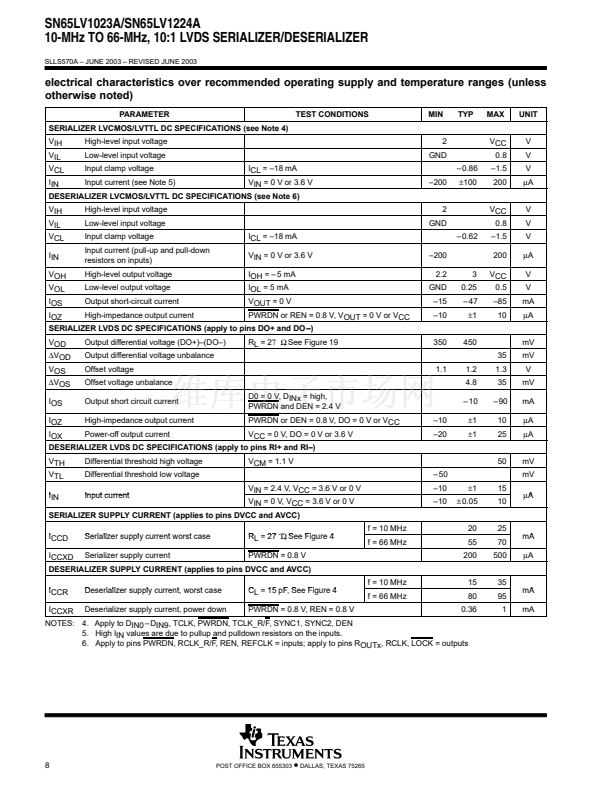 8
8
 9
9
 10
10
 11
11
 12
12
 13
13
 14
14
 15
15
 16
16
 17
17
 18
18
 19
19
 20
20
 21
21
 22
22
