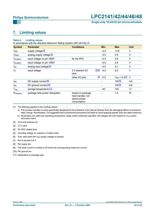
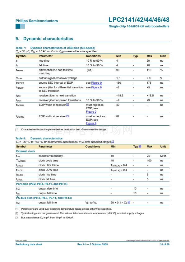
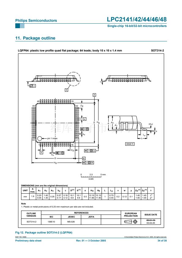
9. Dynamic characteristics
鈩?/div>
on D+ to V
DD
,unless otherwise speci铿乪d
Symbol
t
r
t
f
t
FRFM
V
CRS
t
FEOPT
t
FDEOP
t
JR1
t
JR2
t
EOPR1
Parameter
rise time
fall time
differential rise and fall time
matching
output signal crossover voltage
source SE0 interval of EOP
source jitter for differential transition
to SE0 transition
receiver jitter to next transition
receiver jitter for paired transitions
EOP width at receiver
[1]
10 % to 90 %
must reject as
EOP; see
Figure 9
must accept as
EOP; see
Figure 9
see
Figure 9
see
Figure 9
Conditions
10 % to 90 %
10 % to 90 %
(t
r
/t
f
)
Min
4
4
90
1.3
160
鈭?
鈭?8.5
鈭?
40
Typ
-
-
-
-
-
-
-
-
-
Max
20
20
110
2.0
175
+5
+18.5
+9
-
Unit
ns
ns
%
V
ns
ns
ns
ns
ns
t
EOPR2
EOP width at receiver
[1]
82
-
-
ns
[1]
Characterized but not implemented as production test. Guaranteed by design.
Table 8:
Dynamic characteristics
T
a
=
鈭?/div>
40
掳
C to +85
掳
C for commercial applications, V
DD
over speci铿乪d ranges
[1]
Symbol
External clock
f
osc
T
cy(CLK)
t
CHCX
t
CLCX
t
CLCH
t
CHCL
t
r(o)
t
f(o)
t
f(o)
[1]
[2]
[3]
Parameter
oscillator frequency
clock cycle time
clock HIGH time
clock LOW time
clock rise time
clock fall time
output rise time
output fall time
output fall time
Conditions
Min
10
40
T
cy(CLK)
脳
0.4
T
cy(CLK)
脳
0.4
-
-
-
-
Typ
[2]
-
-
-
-
-
-
10
10
-
Max
25
100
-
-
5
5
-
-
-
Unit
MHz
ns
ns
ns
ns
ns
ns
ns
ns
Port pins (P0.2, P0.3, P0.11, and P0.14)
I
2
C-bus pins (P0.2, P0.3, P0.11, and P0.14)
V
IH
to V
IL
20 + 0.1
脳
C
b
[3]
Parameters are valid over operating temperature range unless otherwise speci铿乪d.
Typical ratings are not guaranteed. The values listed are at room temperature (+25 藲C), nominal supply voltages.
Bus capacitance C
b
in pF, from 10 pF to 400 pF.
9397 750 14985
漏 Koninklijke Philips Electronics N.V. 2005. All rights reserved.
Preliminary data sheet
Rev. 01 鈥?3 October 2005
31 of 38


 1
1
 2
2
 3
3
 4
4
 5
5
 6
6
 7
7
 8
8
 9
9
 10
10
 11
11
 12
12
 13
13
 14
14
 15
15
 16
16
 17
17
 18
18
 19
19
 20
20
 21
21
 22
22
 23
23
 24
24
 25
25
 26
26
 27
27
 28
28
 29
29
 30
30
 31
31
 32
32
 33
33
 34
34
 35
35
 36
36
 37
37
 38
38
