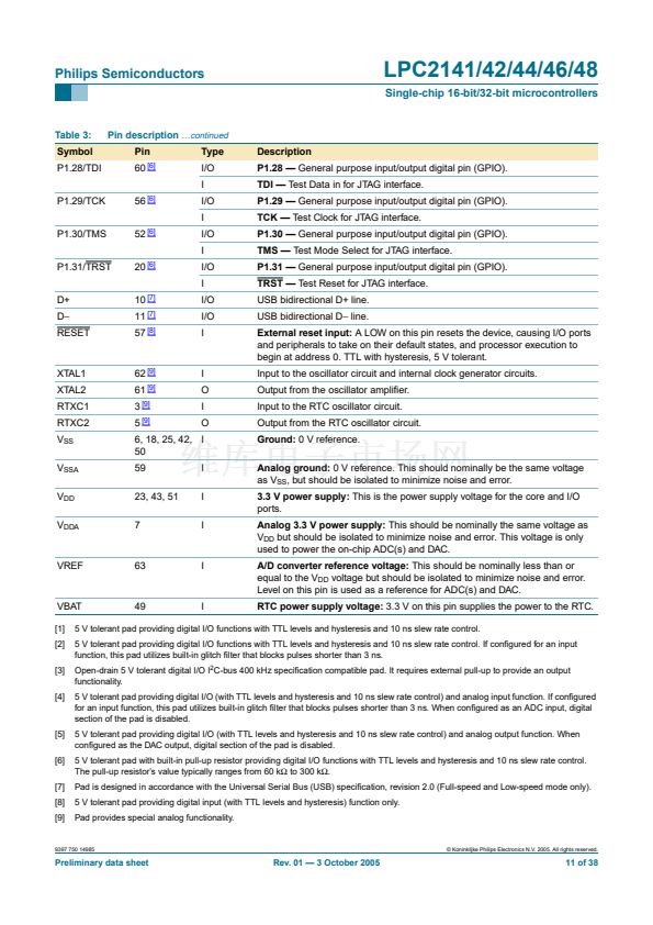
Philips Semiconductors
LPC2141/42/44/46/48
Single-chip 16-bit/32-bit microcontrollers
The Wake-up Timer monitors the crystal oscillator as the means of checking whether it is
safe to begin code execution. When power is applied to the chip, or some event caused
the chip to exit Power-down mode, some time is required for the oscillator to produce a
signal of suf铿乧ient amplitude to drive the clock logic. The amount of time depends on
many factors, including the rate of V
DD
ramp (in the case of power on), the type of crystal
and its electrical characteristics (if a quartz crystal is used), as well as any other external
circuitry (e.g. capacitors), and the characteristics of the oscillator itself under the existing
ambient conditions.
6.19.4 Brownout detector
The LPC2141/42/44/46/48 include 2-stage monitoring of the voltage on the V
DD
pins. If
this voltage falls below 2.9 V, the BOD asserts an interrupt signal to the VIC. This signal
can be enabled for interrupt; if not, software can monitor the signal by reading dedicated
register.
The second stage of low voltage detection asserts reset to inactivate the
LPC2141/42/44/46/48 when the voltage on the V
DD
pins falls below 2.6 V. This reset
prevents alteration of the 铿俛sh as operation of the various elements of the chip would
otherwise become unreliable due to low voltage. The BOD circuit maintains this reset
down below 1 V, at which point the POR circuitry maintains the overall reset.
Both the 2.9 V and 2.6 V thresholds include some hysteresis. In normal operation, this
hysteresis allows the 2.9 V detection to reliably interrupt, or a regularly-executed event
loop to sense the condition.
6.19.5 Code security
This feature of the LPC2141/42/44/46/48 allow an application to control whether it can be
debugged or protected from observation.
If after reset on-chip boot loader detects a valid checksum in 铿俛sh and reads 0x8765 4321
from address 0x1FC in 铿俛sh, debugging will be disabled and thus the code in 铿俛sh will be
protected from observation. Once debugging is disabled, it can be enabled only by
performing a full chip erase using the ISP.
6.19.6 External interrupt inputs
The LPC2141/42/44/46/48 include up to nine edge or level sensitive External Interrupt
Inputs as selectable pin functions. When the pins are combined, external events can be
processed as four independent interrupt signals. The External Interrupt Inputs can
optionally be used to wake-up the processor from Power-down mode.
Additionally capture input pins can also be used as external interrupts without the option
to wake the device up from Power-down mode.
6.19.7 Memory mapping control
The Memory Mapping Control alters the mapping of the interrupt vectors that appear
beginning at address 0x0000 0000. Vectors may be mapped to the bottom of the on-chip
铿俛sh memory, or to the on-chip static RAM. This allows code running in different memory
spaces to have control of the interrupts.
9397 750 14985
漏 Koninklijke Philips Electronics N.V. 2005. All rights reserved.
Preliminary data sheet
Rev. 01 鈥?3 October 2005
22 of 38


 1
1
 2
2
 3
3
 4
4
 5
5
 6
6
 7
7
 8
8
 9
9
 10
10
 11
11
 12
12
 13
13
 14
14
 15
15
 16
16
 17
17
 18
18
 19
19
 20
20
 21
21
 22
22
 23
23
 24
24
 25
25
 26
26
 27
27
 28
28
 29
29
 30
30
 31
31
 32
32
 33
33
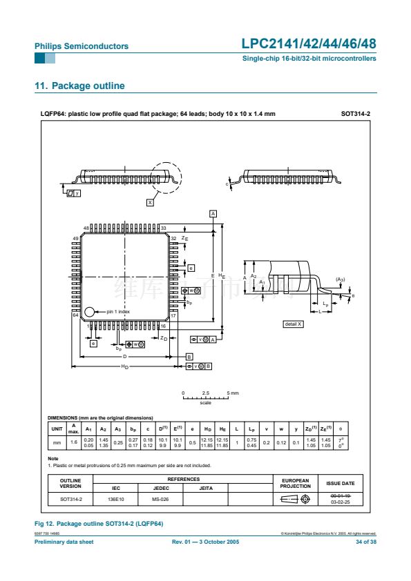 34
34
 35
35
 36
36
 37
37
 38
38
