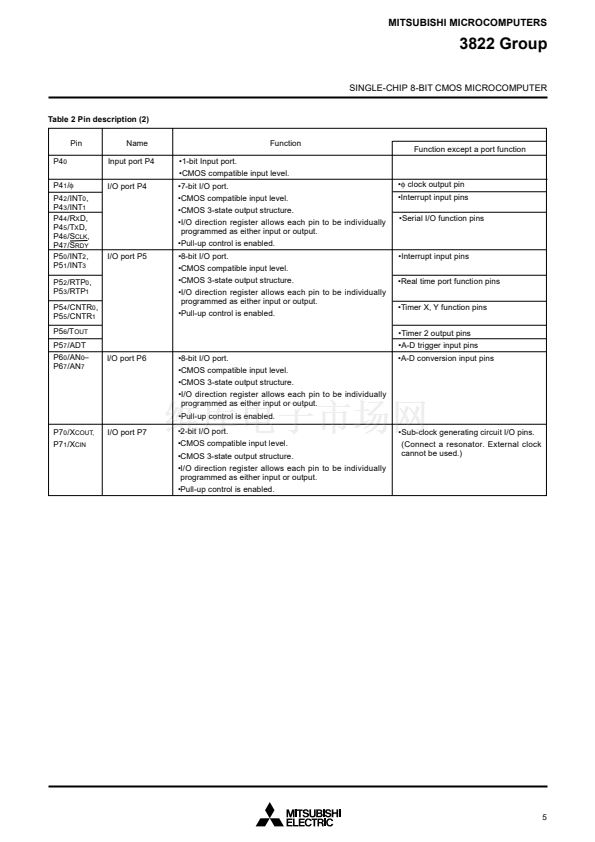
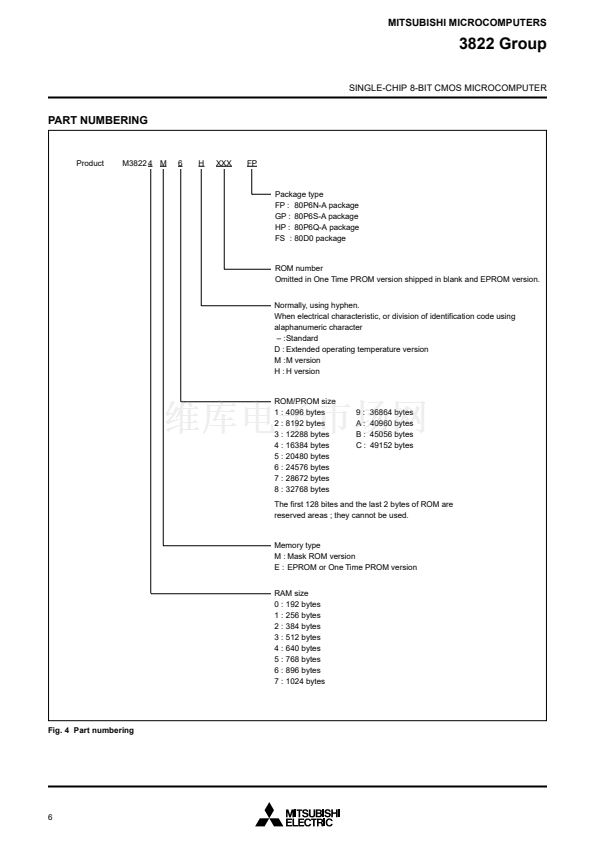
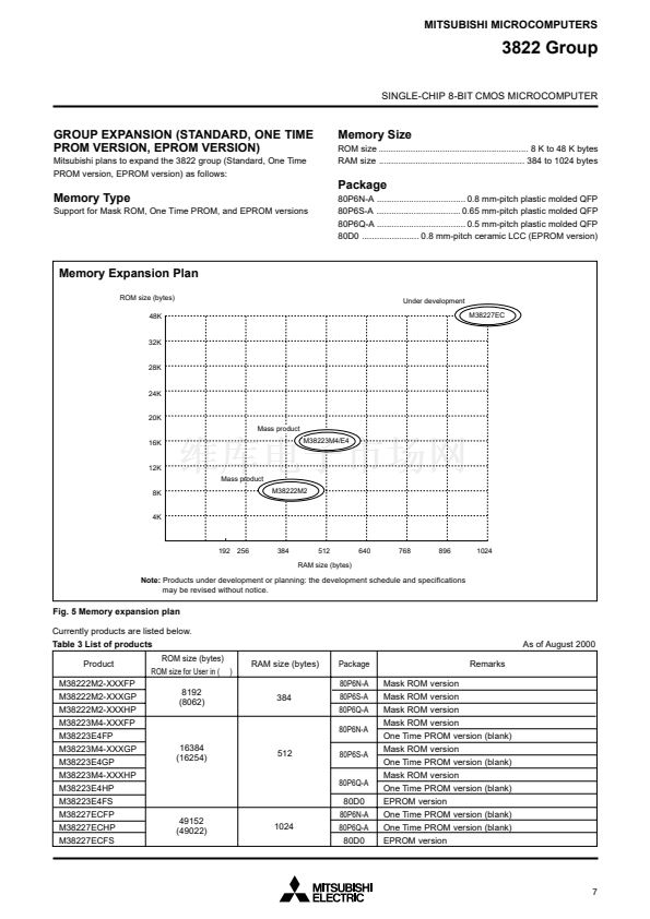
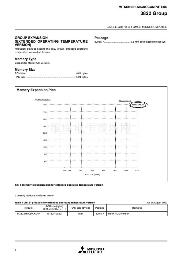
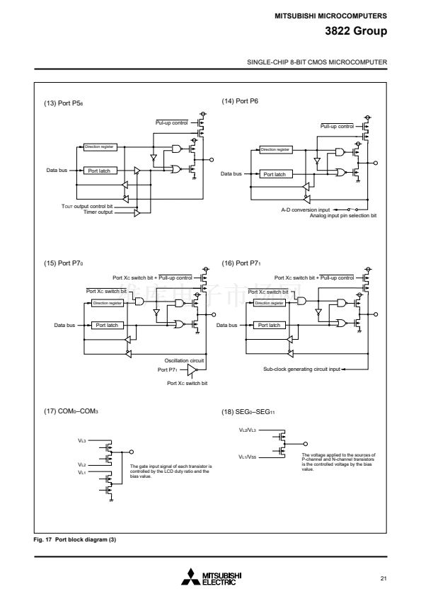
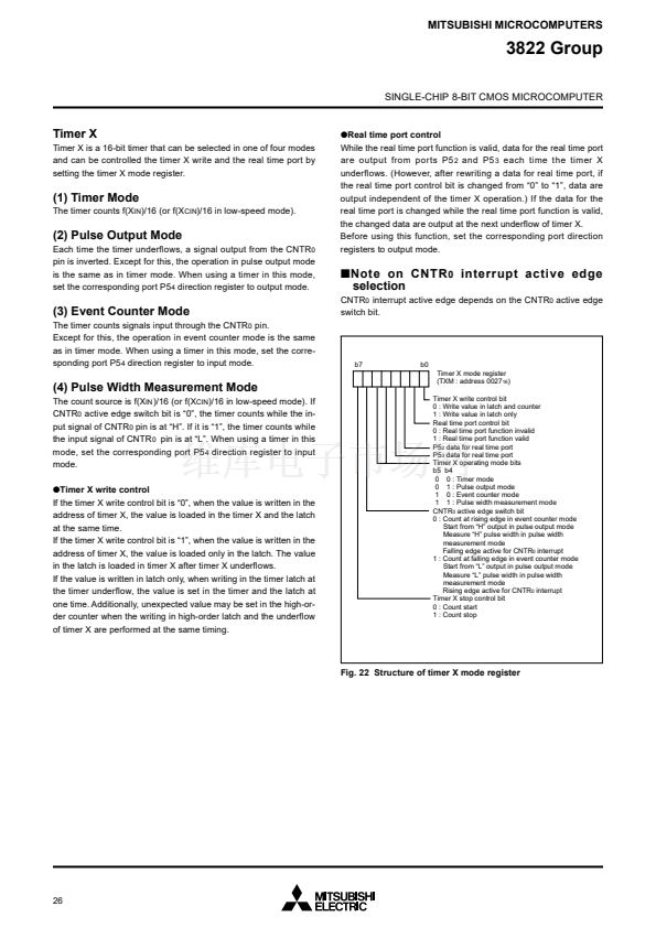
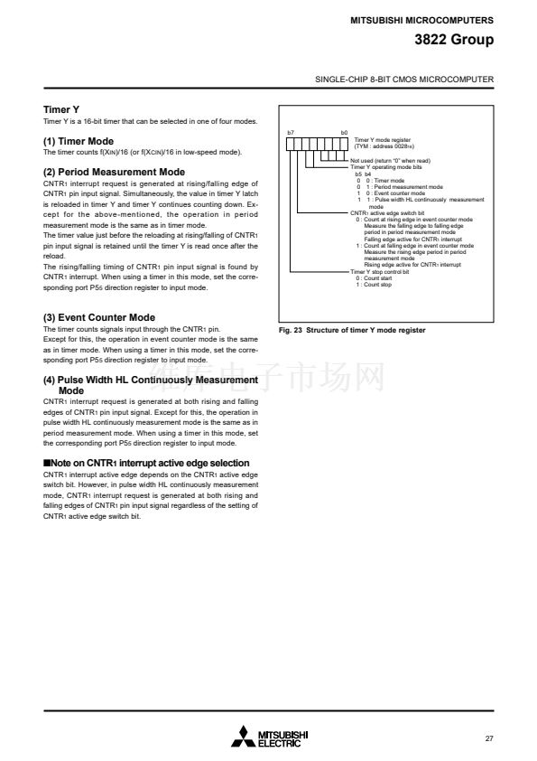
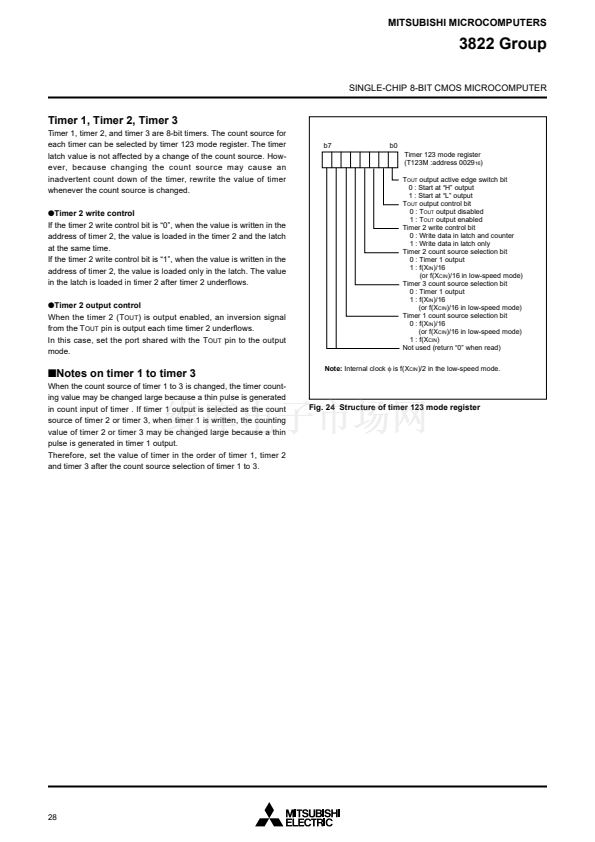
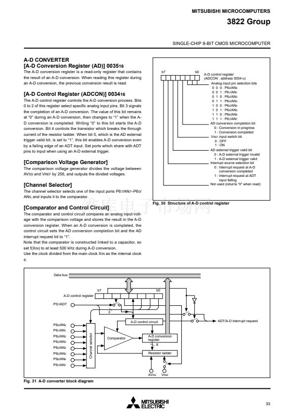
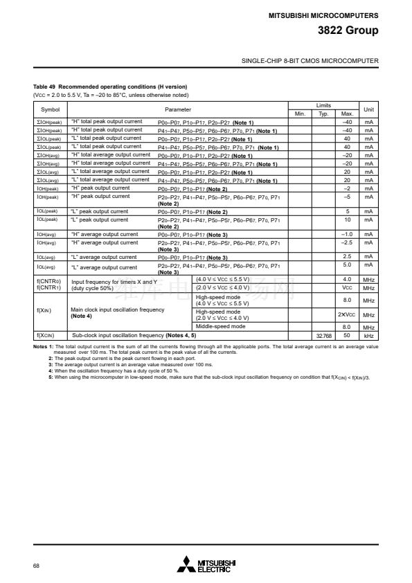
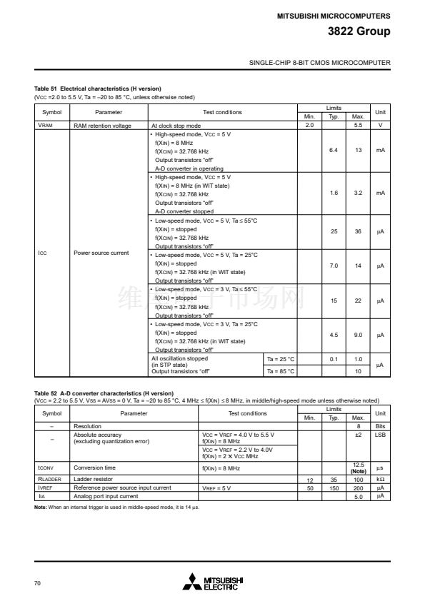
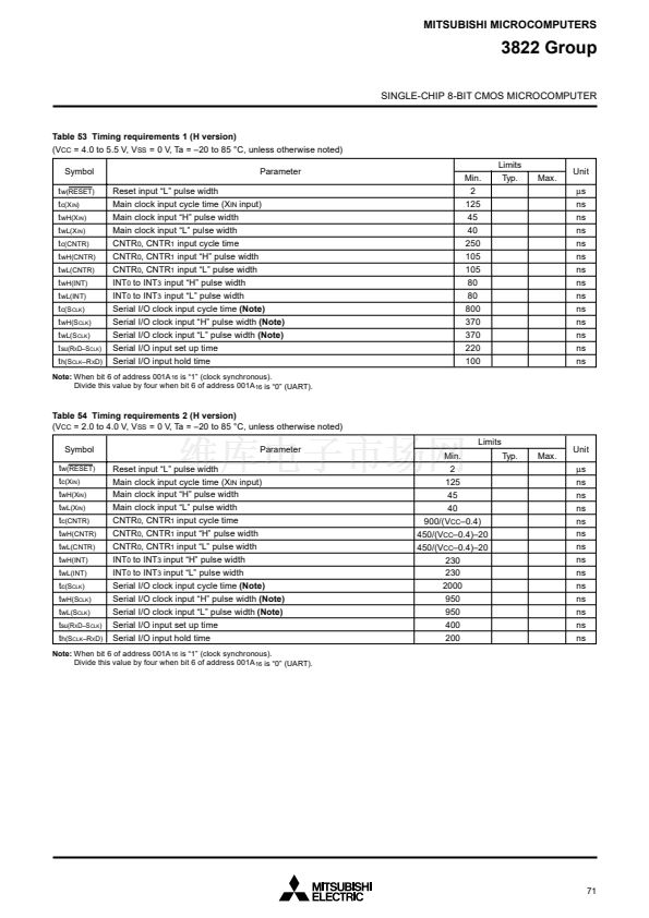
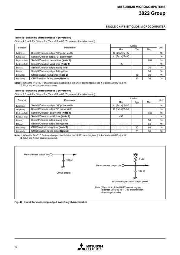
MITSUBISHI MICROCOMPUTERS
3822 Group
SINGLE-CHIP 8-BIT CMOS MICROCOMPUTER
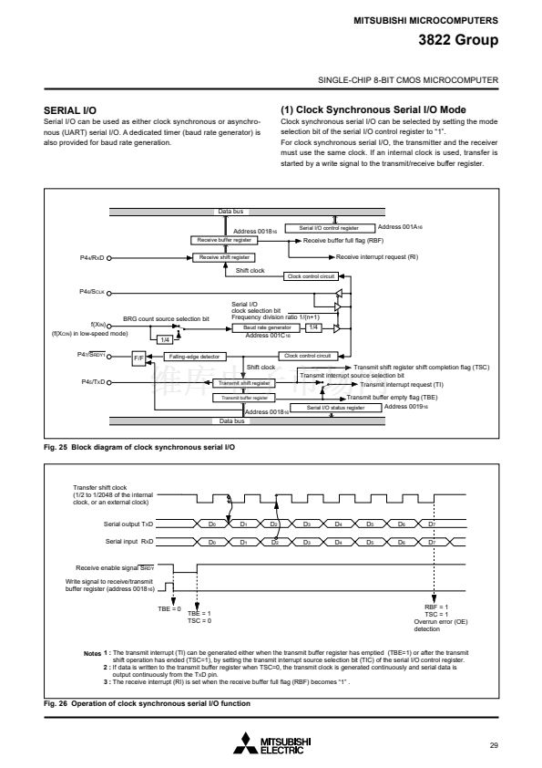
SERIAL I/O
Serial I/O can be used as either clock synchronous or asynchro-
nous (UART) serial I/O. A dedicated timer (baud rate generator) is
also provided for baud rate generation.
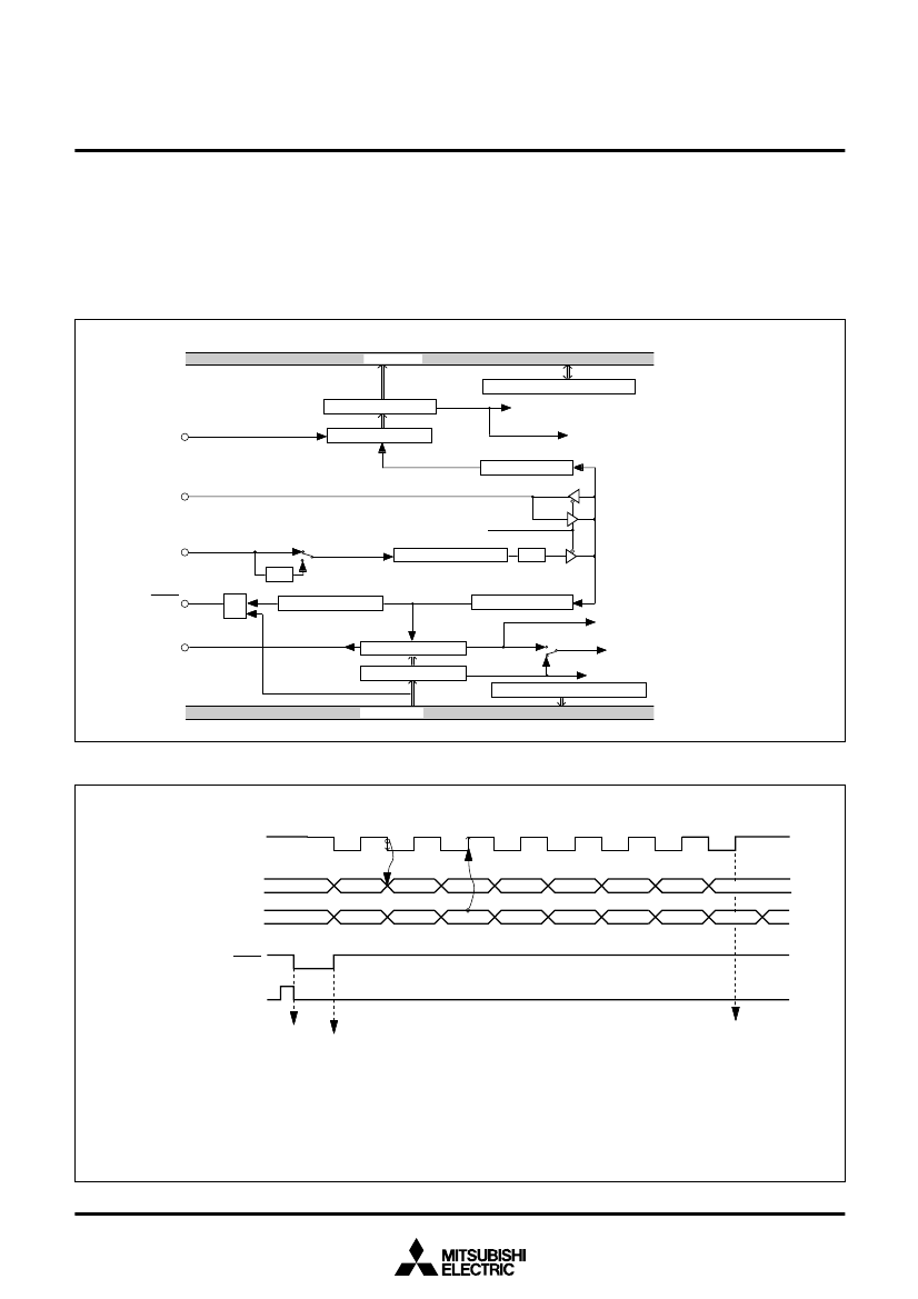
(1) Clock Synchronous Serial I/O Mode
Clock synchronous serial I/O can be selected by setting the mode
selection bit of the serial I/O control register to 鈥?鈥?
For clock synchronous serial I/O, the transmitter and the receiver
must use the same clock. If an internal clock is used, transfer is
started by a write signal to the transmit/receive buffer register.
Data bus
Address 0018
16
Receive buffer register
Serial I/O control register
Address 001A
16
Receive buffer full flag (RBF)
Receive interrupt request (RI)
Clock control circuit
P4
4
/R
X
D
Receive shift register
Shift clock
P4
6
/S
CLK
Serial I/O
clock selection bit
Frequency division ratio 1/(n+1)
Baud rate generator
BRG count source selection bit
f(X
IN
)
(f(X
CIN
) in low-speed mode)
1/4
P4
7
/S
RDY1
F/F
Falling-edge detector
1/4
Address 001C
16
Clock control circuit
Shift clock
P4
5
/T
X
D
Transmit shift register
Transmit buffer register
Transmit shift register shift completion flag (TSC)
Transmit interrupt source selection bit
Transmit interrupt request (TI)
Transmit buffer empty flag (TBE)
Address 0019
16
Address 0018
16
Data bus
Serial I/O status register
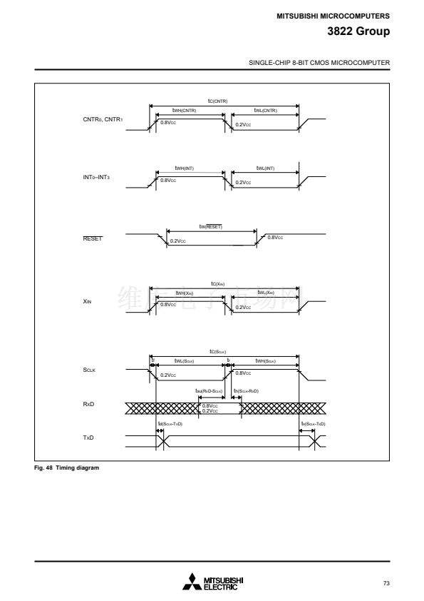
Fig. 25 Block diagram of clock synchronous serial I/O
Transfer shift clock
(1/2 to 1/2048 of the internal
clock, or an external clock)
D
0
D
0
D
1
D
1
D
2
D
2
D
3
D
3
D
4
D
4
D
5
D
5
D
6
D
6
D
7
D
7
Serial output T
X
D
Serial input R
X
D
Receive enable signal S
RDY
Write signal to receive/transmit
buffer register (address 0018
16
)
TBE = 0
RBF = 1
TSC = 1
Overrun error (OE)
detection
TBE = 1
TSC = 0
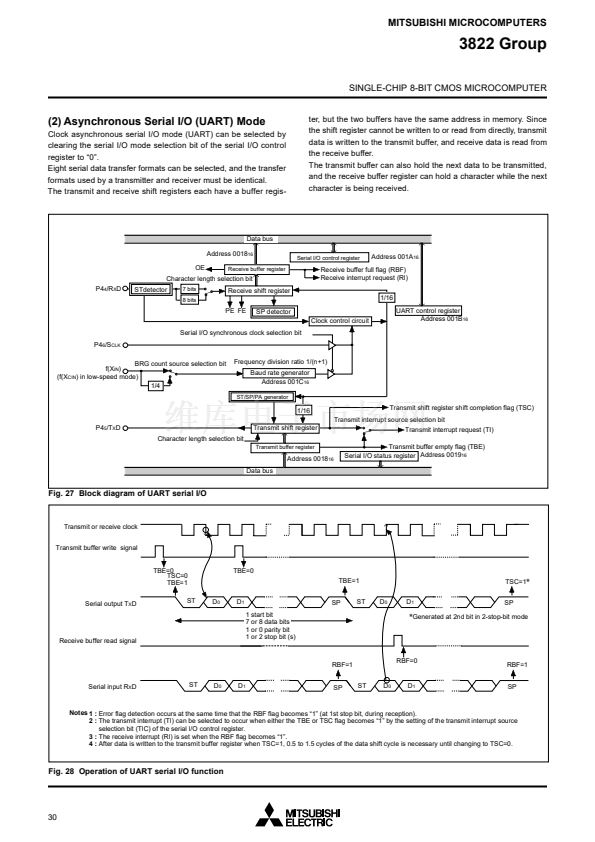
Notes 1 :
T he transmit interrupt (TI) can be generated either when the transmit buffer register has emptied (TBE=1) or after the transmit
shift operation has ended (TSC=1), by setting the transmit interrupt source selection bit (TIC) of the serial I/O control register.
2 :
If data is written to the transmit buffer register when TSC=0, the transmit clock is generated continuously and serial data is
output continuously from the T
X
D pin.
3 :
T he receive interrupt (RI) is set when the receive buffer full flag (RBF) becomes 鈥?鈥?.
Fig. 26 Operation of clock synchronous serial I/O function
29


 1
1
 2
2
 3
3
 4
4
 5
5
 6
6
 7
7
 8
8
 9
9
 10
10
 11
11
 12
12
 13
13
 14
14
 15
15
 16
16
 17
17
 18
18
 19
19
 20
20
 21
21
 22
22
 23
23
 24
24
 25
25
 26
26
 27
27
 28
28
 29
29
 30
30
 31
31
 32
32
 33
33
 34
34
 35
35
 36
36
 37
37
 38
38
 39
39
 40
40
 41
41
 42
42
 43
43
 44
44
 45
45
 46
46
 47
47
 48
48
 49
49
 50
50
 51
51
 52
52
 53
53
 54
54
 55
55
 56
56
 57
57
 58
58
 59
59
 60
60
 61
61
 62
62
 63
63
 64
64
 65
65
 66
66
 67
67
 68
68
 69
69
 70
70
 71
71
 72
72
 73
73
 74
74
 75
75
 76
76
 77
77
 78
78
