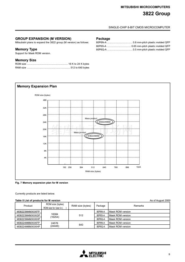
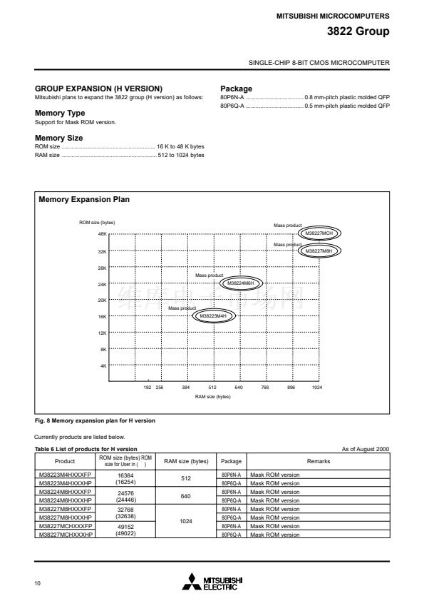
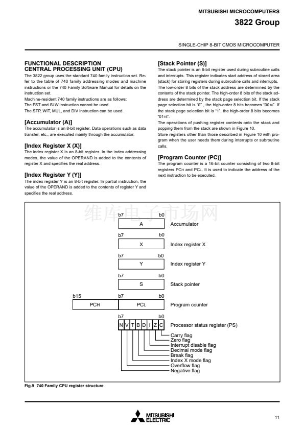
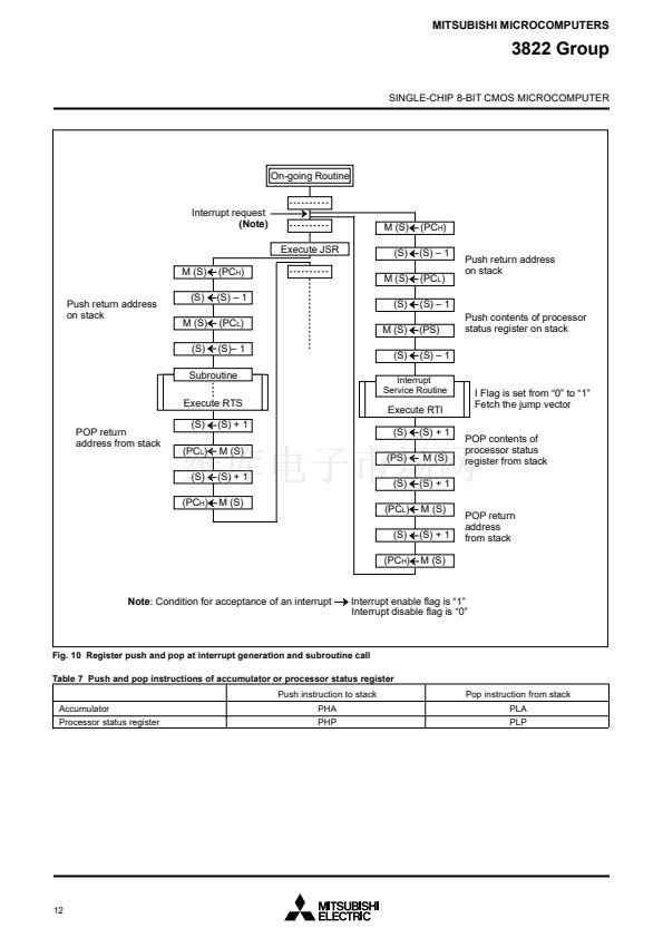
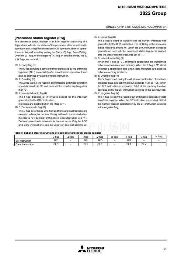
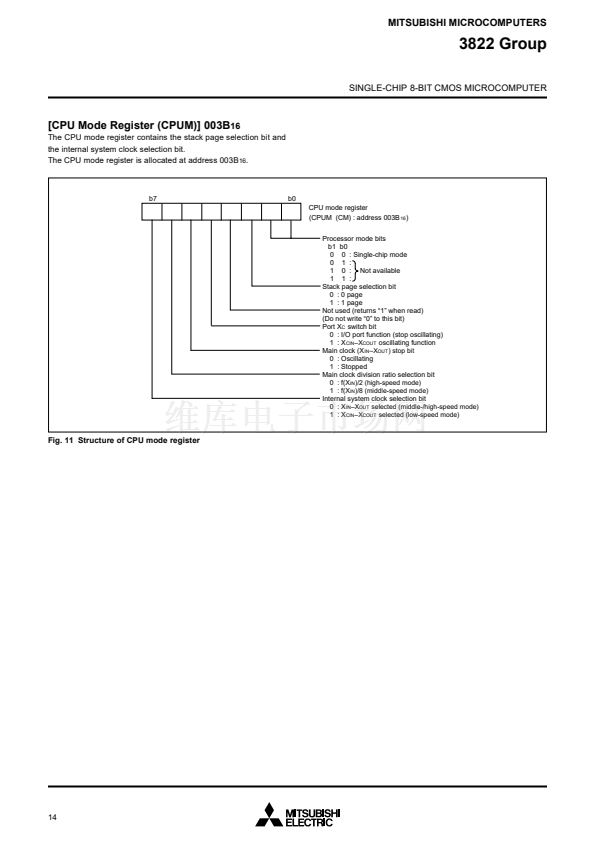
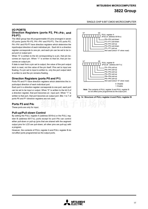
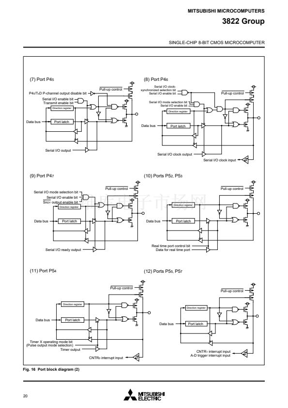
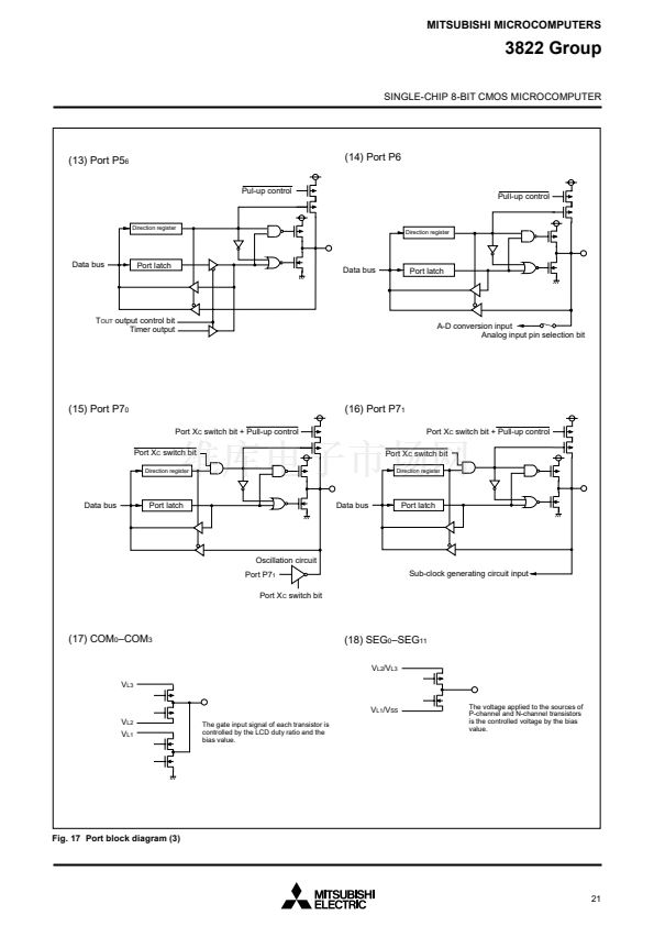
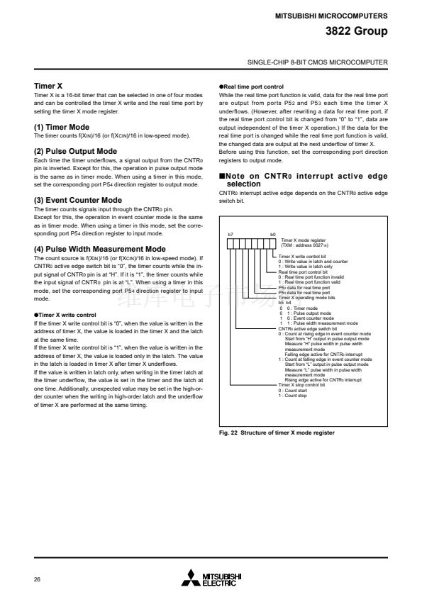
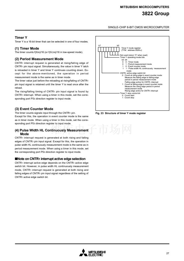
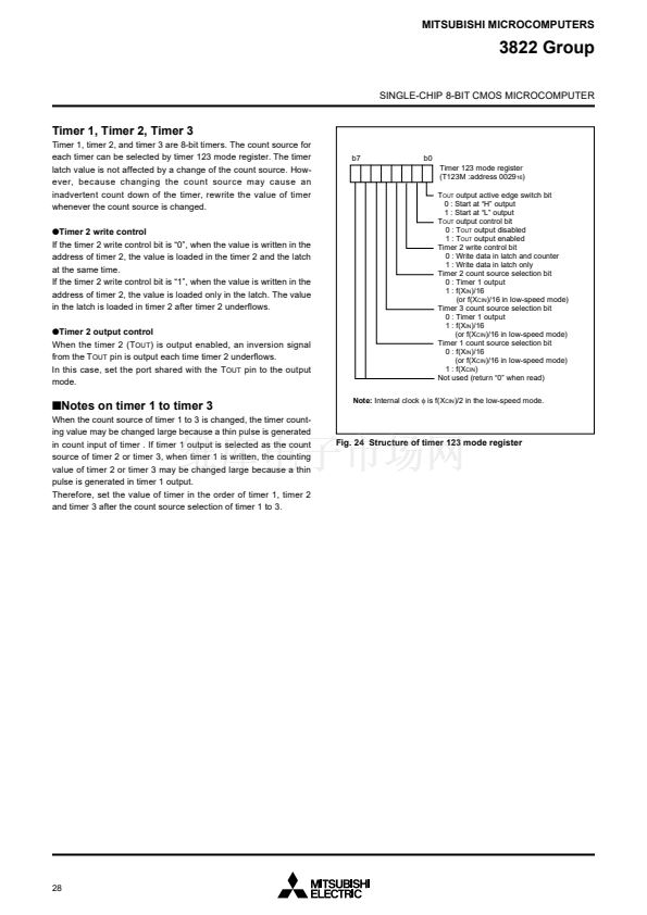
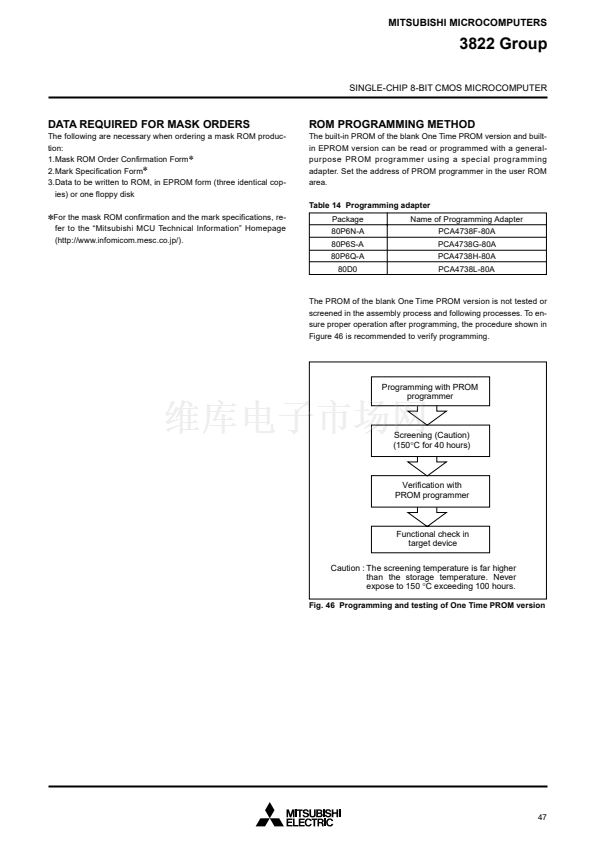
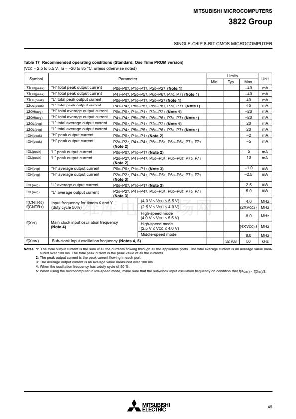
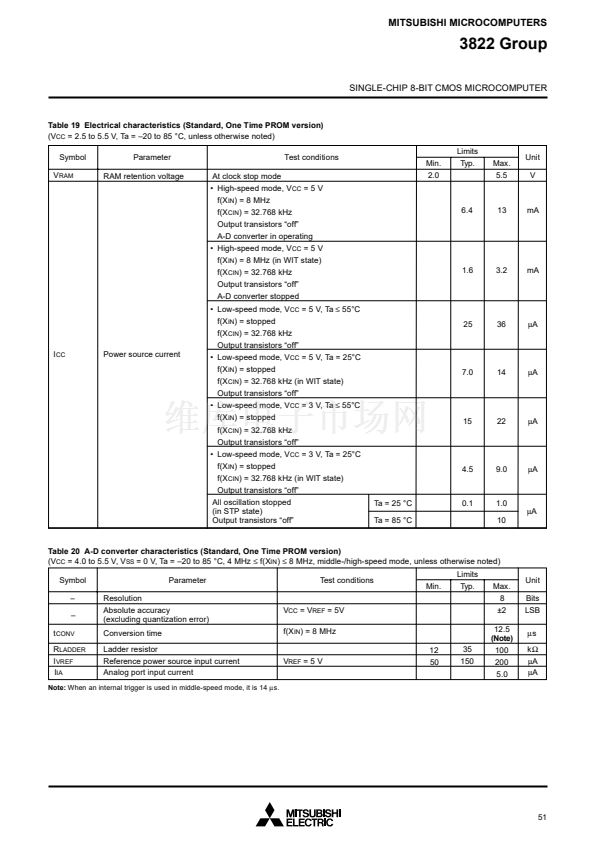
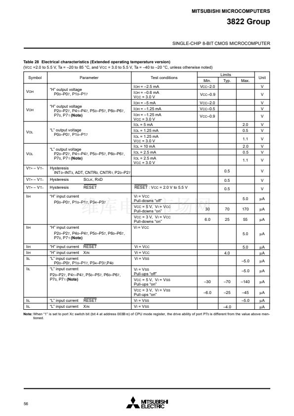
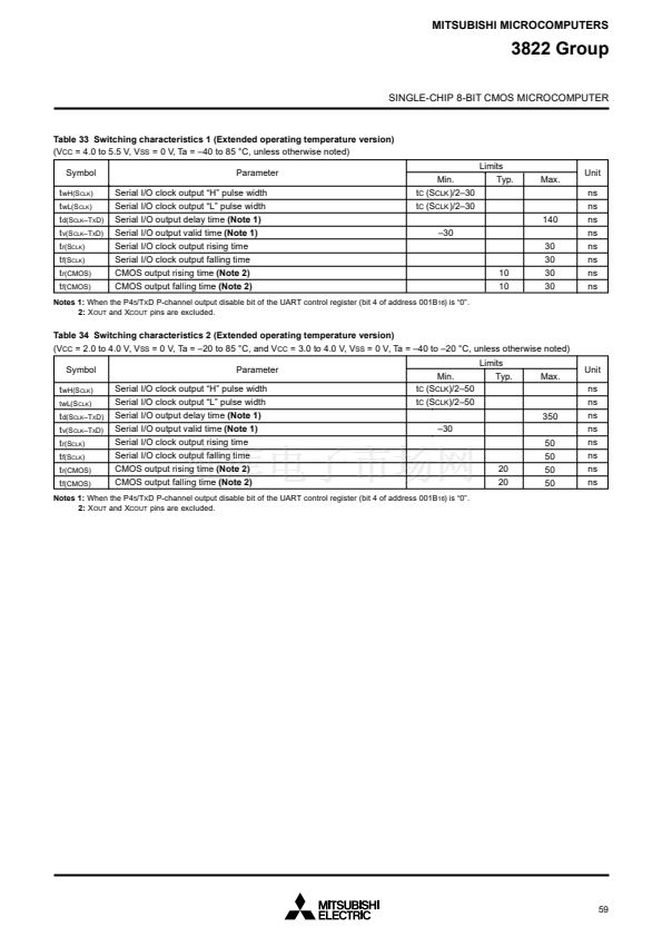
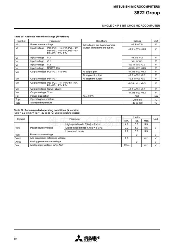
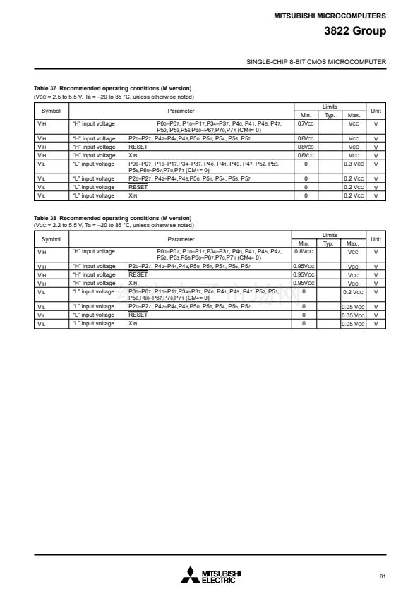
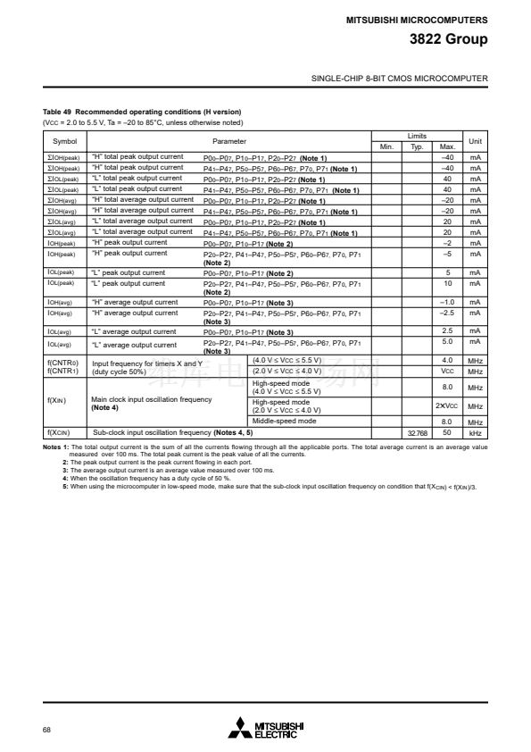
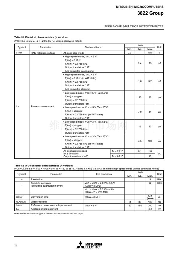
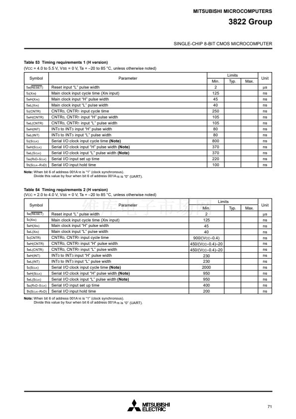
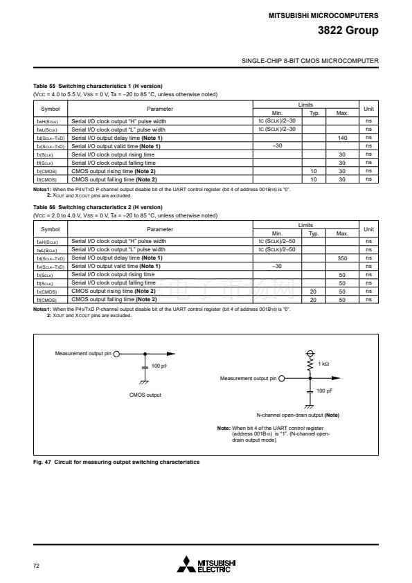
MITSUBISHI MICROCOMPUTERS
3822 Group
SINGLE-CHIP 8-BIT CMOS MICROCOMPUTER
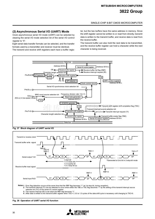
(2) Asynchronous Serial I/O (UART) Mode
Clock asynchronous serial I/O mode (UART) can be selected by
clearing the serial I/O mode selection bit of the serial I/O control
register to 鈥?鈥?
Eight serial data transfer formats can be selected, and the transfer
formats used by a transmitter and receiver must be identical.
The transmit and receive shift registers each have a buffer regis-
ter, but the two buffers have the same address in memory. Since
the shift register cannot be written to or read from directly, transmit
data is written to the transmit buffer, and receive data is read from
the receive buffer.
The transmit buffer can also hold the next data to be transmitted,
and the receive buffer register can hold a character while the next
character is being received.
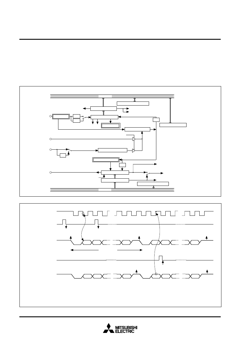
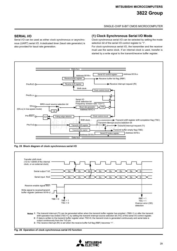
Data bus
Address 0018
16
OE
P4
4
/R
X
D
STdetector
7 bits
8 bits
Receive buffer register
Serial I/O control register
Address 001A
16
Character length selection bit
Receive shift register
Receive buffer full flag (RBF)
Receive interrupt request (RI)
1/16
PE FE
SP detector
Clock control circuit
UART control register
Address 001B
16
Serial I/O synchronous clock selection bit
P4
6
/S
CLK
BRG count source selection bit
f(X
IN
)
(f(X
CIN
) in low-speed mode)
1/4
Frequency division ratio 1/(n+1)
Baud rate generator
Address 001C
16
ST/SP/PA generator
1/16
P4
5
/T
X
D
Character length selection bit
Transmit buffer register
Transmit shift register shift completion flag (TSC)
Transmit interrupt source selection bit
Transmit interrupt request (TI)
Transmit buffer empty flag (TBE)
Serial I/O status register Address 0019
16
Transmit shift register
Address 0018
16
Data bus
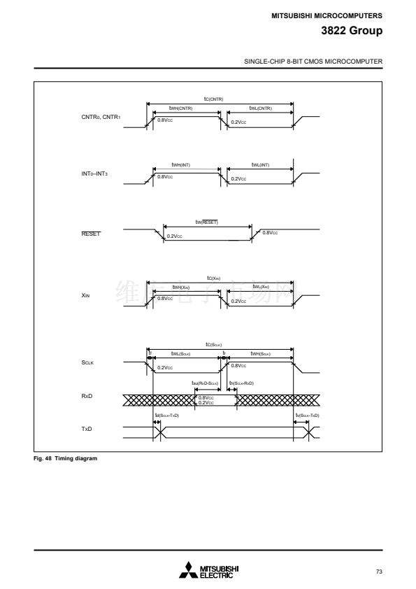
Fig. 27 Block diagram of UART serial I/O
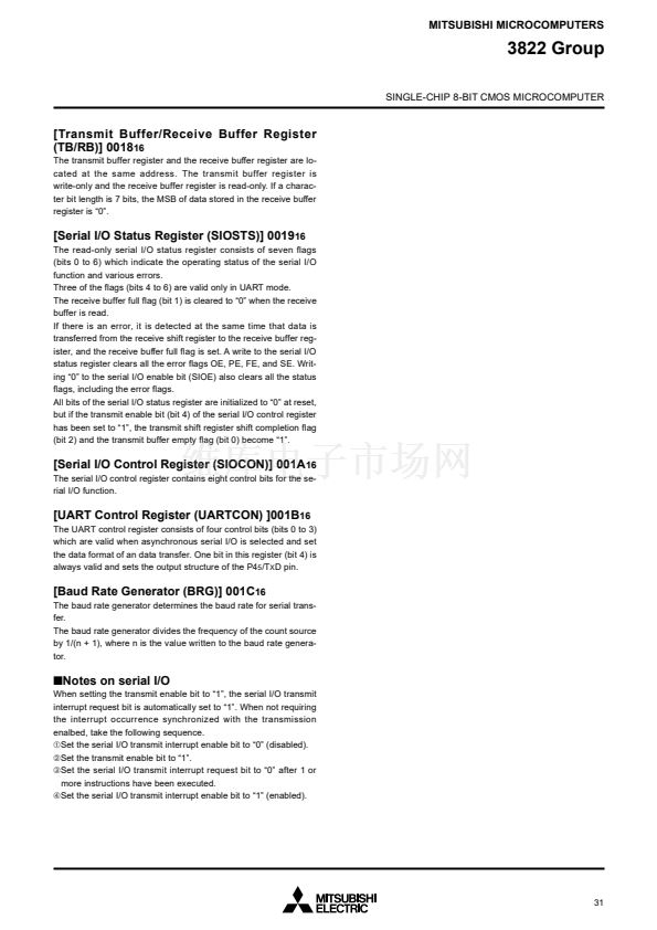
Transmit or receive clock
Transmit buffer write signal
TBE=0
TSC=0
TBE=1
Serial output T
X
D
ST
D
0
TBE=0
TBE=1
D
1
1 start bit
7 or 8 data bits
1 or 0 parity bit
1 or 2 stop bit (s)
SP
ST
D
0
D
1
锟?frac12;
Generated
TSC=1
锟?frac12;
SP
at 2nd bit in 2-stop-bit mode
Receive buffer read signal
RBF=1
Serial input R
X
D
ST
D
0
D
1
ST
D
0
RBF=0
RBF=1
SP
SP
D
1
Notes 1 :
Error flag detection occurs at the same time that the RBF flag becomes 鈥?鈥?(at 1st stop bit, during reception).
2 :
The transmit interrupt (TI) can be selected to occur when either the TBE or TSC flag becomes 鈥?鈥?by the setting of the transmit interrupt source
selection bit (TIC) of the serial I/O control register.
3 :
The receive interrupt (RI) is set when the RBF flag becomes 鈥?鈥?
4 :
After data is written to the transmit buffer register when TSC=1, 0.5 to 1.5 cycles of the data shift cycle is necessary until changing to TSC=0.
Fig. 28 Operation of UART serial I/O function
30


 1
1
 2
2
 3
3
 4
4
 5
5
 6
6
 7
7
 8
8
 9
9
 10
10
 11
11
 12
12
 13
13
 14
14
 15
15
 16
16
 17
17
 18
18
 19
19
 20
20
 21
21
 22
22
 23
23
 24
24
 25
25
 26
26
 27
27
 28
28
 29
29
 30
30
 31
31
 32
32
 33
33
 34
34
 35
35
 36
36
 37
37
 38
38
 39
39
 40
40
 41
41
 42
42
 43
43
 44
44
 45
45
 46
46
 47
47
 48
48
 49
49
 50
50
 51
51
 52
52
 53
53
 54
54
 55
55
 56
56
 57
57
 58
58
 59
59
 60
60
 61
61
 62
62
 63
63
 64
64
 65
65
 66
66
 67
67
 68
68
 69
69
 70
70
 71
71
 72
72
 73
73
 74
74
 75
75
 76
76
 77
77
 78
78
