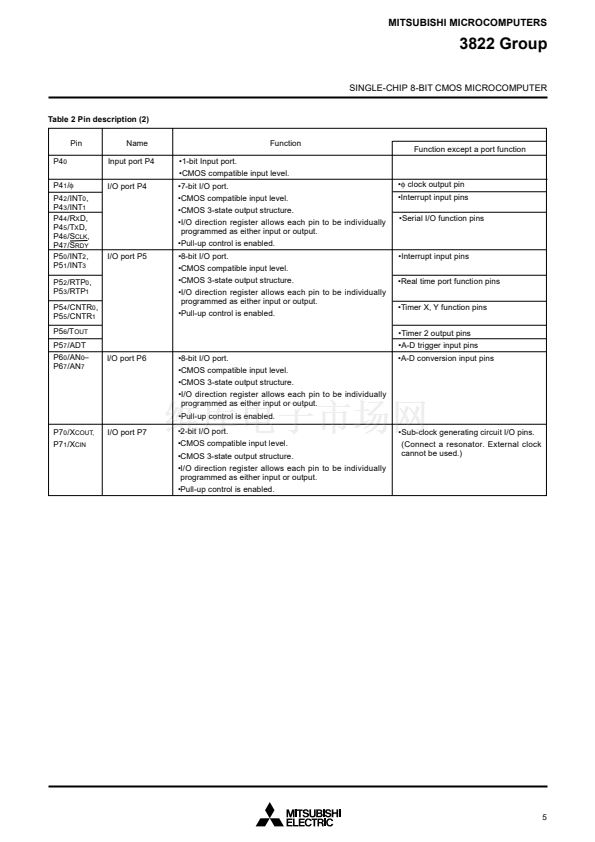
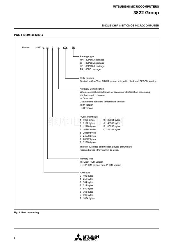
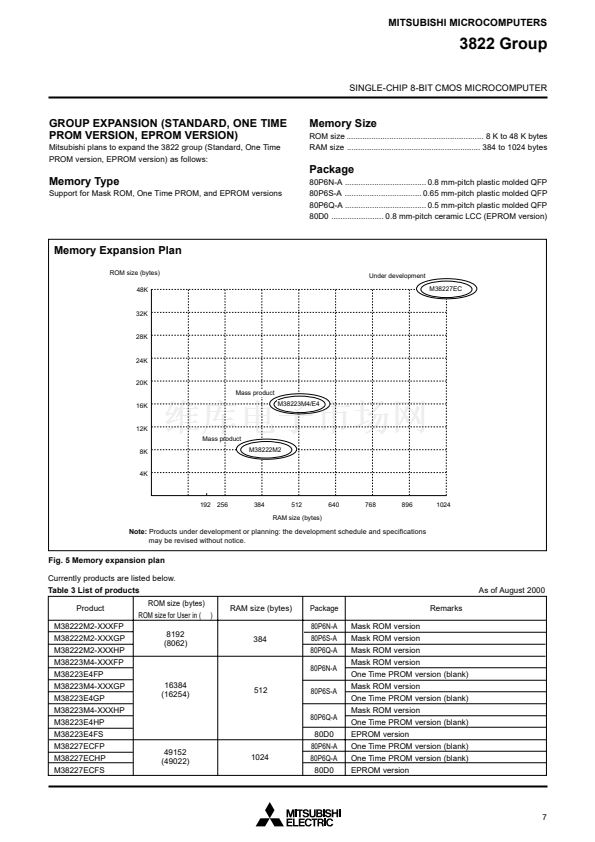
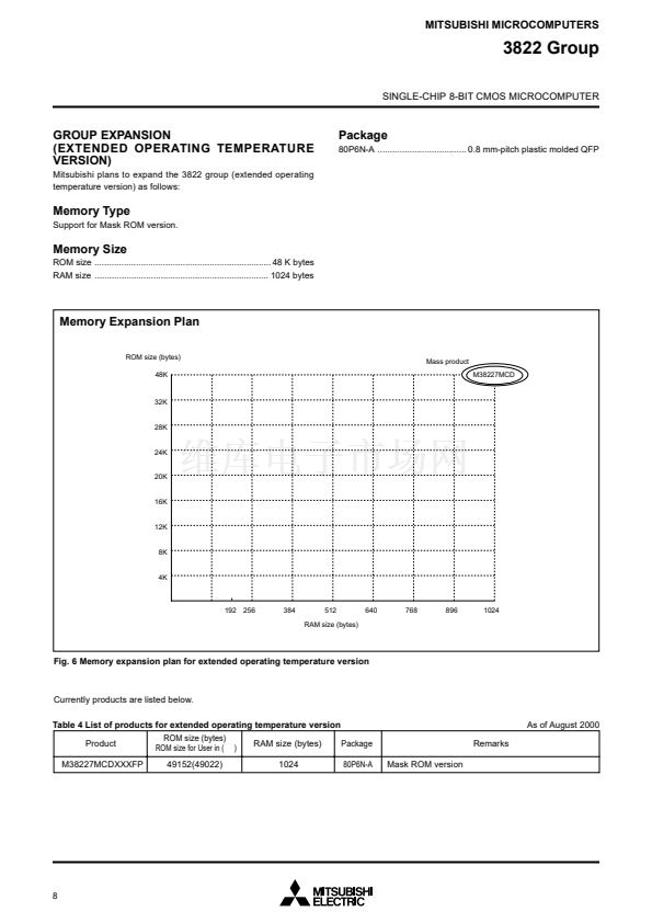
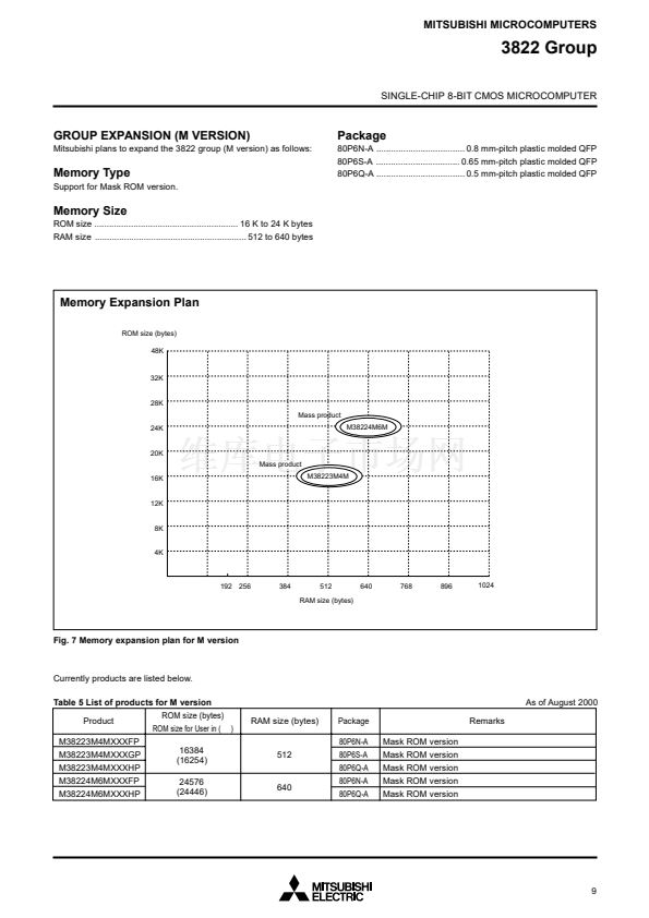
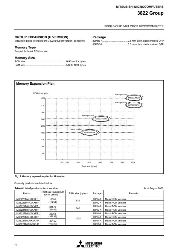
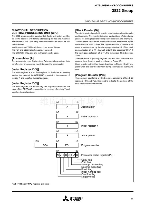
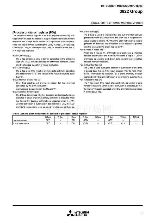
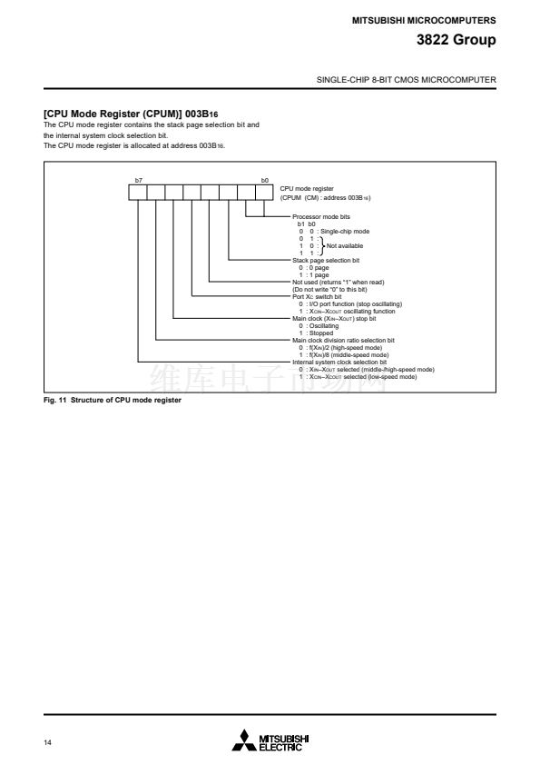
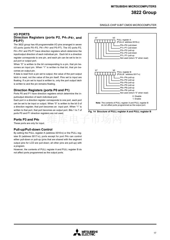
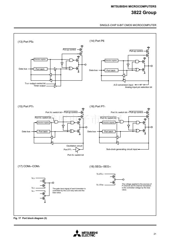
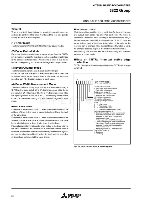
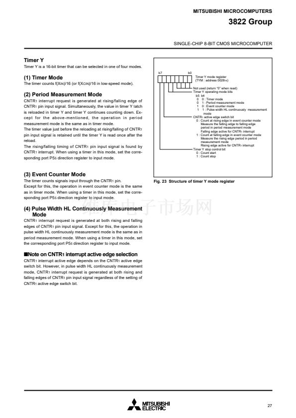
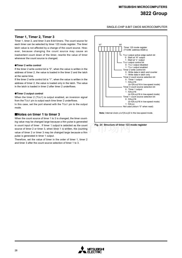
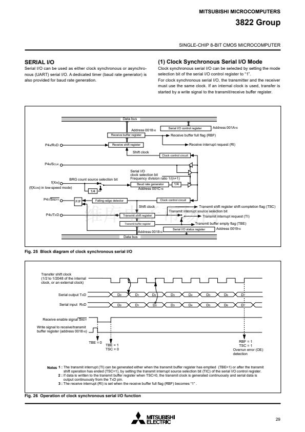
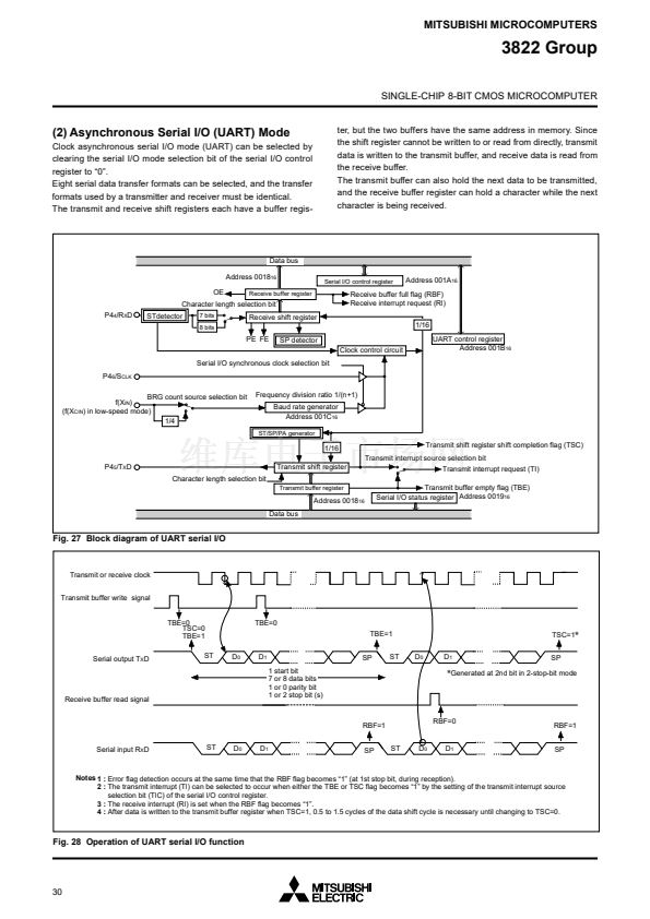
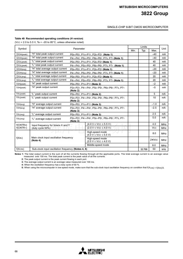
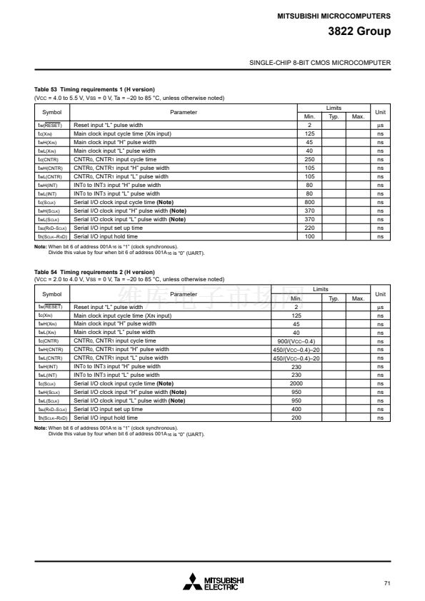
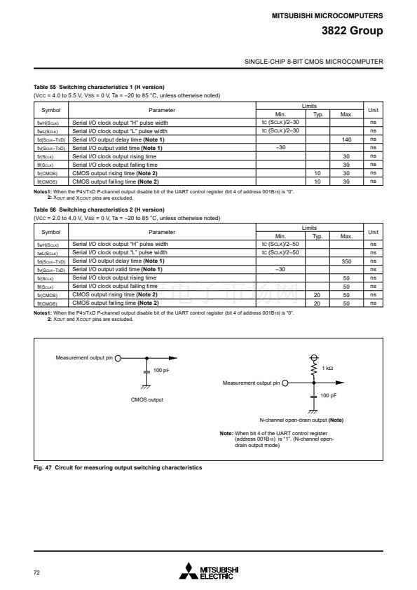
MITSUBISHI MICROCOMPUTERS
3822 Group
SINGLE-CHIP 8-BIT CMOS MICROCOMPUTER
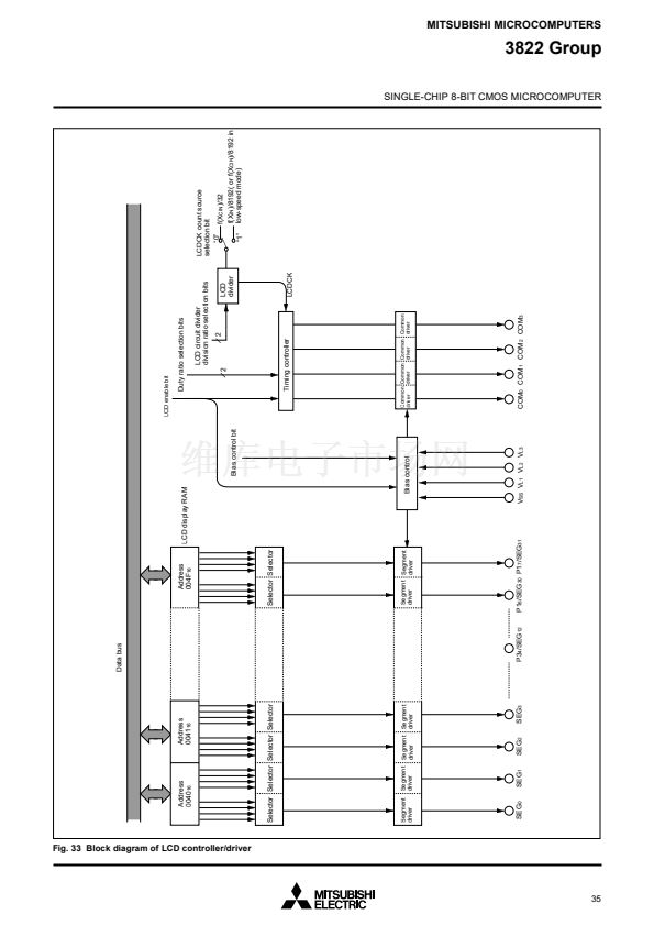
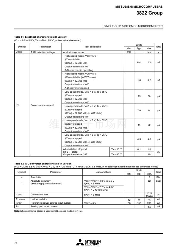
A-D CONVERTER
[A-D Conversion Register (AD)] 0035
16
The A-D conversion register is a read-only register that contains
the result of an A-D conversion. When reading this register during
an A-D conversion, the previous conversion result is read.
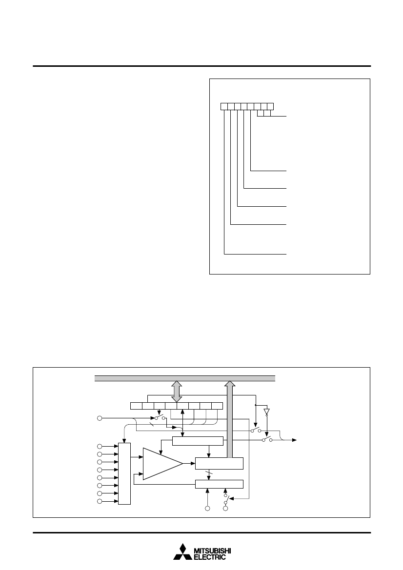
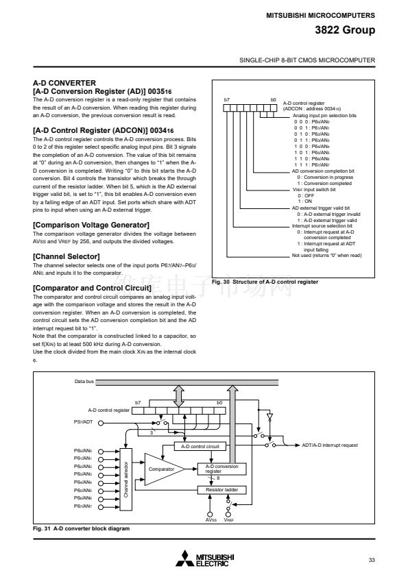
b7
b0
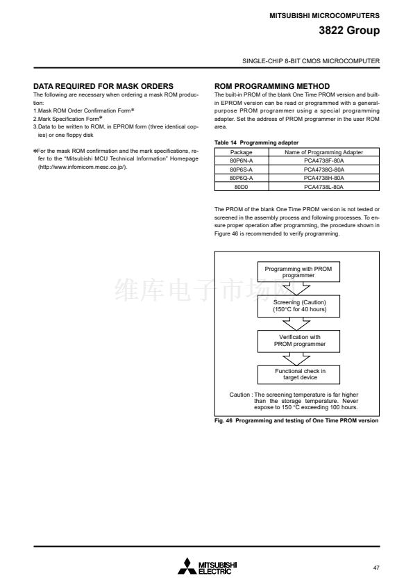
A-D control register
(ADCON : address 0034
16
)
Analog input pin selection bits
0 0 0 : P6
0
/AN
0
0 0 1 : P6
1
/AN
1
0 1 0 : P6
2
/AN
2
0 1 1 : P6
3
/AN
3
1 0 0 : P6
4
/AN
4
1 0 1 : P6
5
/AN
5
1 1 0 : P6
6
/AN
6
1 1 1 : P6
7
/AN
7
AD conversion completion bit
0 : Conversion in progress
1 : Conversion completed
V
REF
input switch bit
0 : OFF
1 : ON
AD external trigger valid bit
0 : A-D external trigger invalid
1 : A-D external trigger valid
Interrupt source selection bit
0 : Interrupt request at A-D
conversion completed
1 : Interrupt request at ADT
input falling
Not used (returns 鈥?鈥?when read)
[A-D Control Register (ADCON)] 0034
16
The A-D control register controls the A-D conversion process. Bits
0 to 2 of this register select specific analog input pins. Bit 3 signals
the completion of an A-D conversion. The value of this bit remains
at 鈥?鈥?during an A-D conversion, then changes to 鈥?鈥?when the A-
D conversion is completed. Writing 鈥?鈥?to this bit starts the A-D
conversion. Bit 4 controls the transistor which breaks the through
current of the resistor ladder. When bit 5, which is the AD external
trigger valid bit, is set to 鈥?鈥? this bit enables A-D conversion even
by a falling edge of an ADT input. Set ports which share with ADT
pins to input when using an A-D external trigger.
[Comparison Voltage Generator]
The comparison voltage generator divides the voltage between
AV
SS
and V
REF
by 256, and outputs the divided voltages.
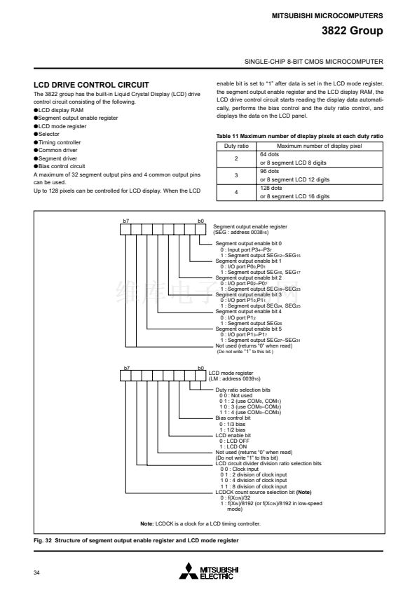
[Channel Selector]
The channel selector selects one of the input ports P6
7
/AN
7
鈥揚6
0
/
AN
0,
and inputs it to the comparator.
Fig. 30 Structure of A-D control register
[Comparator and Control Circuit]
The comparator and control circuit compares an analog input volt-
age with the comparison voltage and stores the result in the A-D
conversion register. When an A-D conversion is completed, the
control circuit sets the AD conversion completion bit and the AD
interrupt request bit to 鈥?鈥?
Note that the comparator is constructed linked to a capacitor, so
set f(X
IN
) to at least 500 kHz during A-D conversion.
Use the clock divided from the main clock X
IN
as the internal clock
蠁.
Data bus
b7
A-D control register
P5
7
/ADT
3
b0
P6
0
/AN
0
P6
1
/AN
1
P6
2
/AN
2
P6
3
/AN
3
P6
4
/AN
4
P6
5
/AN
5
P6
6
/AN
6
P6
7
/AN
7
Channel selector
Comparator
A-D control circuit
ADT/A-D interrupt request
A-D conversion
register
8
Resistor ladder
AV
SS
V
REF
Fig. 31 A-D converter block diagram
33


 1
1
 2
2
 3
3
 4
4
 5
5
 6
6
 7
7
 8
8
 9
9
 10
10
 11
11
 12
12
 13
13
 14
14
 15
15
 16
16
 17
17
 18
18
 19
19
 20
20
 21
21
 22
22
 23
23
 24
24
 25
25
 26
26
 27
27
 28
28
 29
29
 30
30
 31
31
 32
32
 33
33
 34
34
 35
35
 36
36
 37
37
 38
38
 39
39
 40
40
 41
41
 42
42
 43
43
 44
44
 45
45
 46
46
 47
47
 48
48
 49
49
 50
50
 51
51
 52
52
 53
53
 54
54
 55
55
 56
56
 57
57
 58
58
 59
59
 60
60
 61
61
 62
62
 63
63
 64
64
 65
65
 66
66
 67
67
 68
68
 69
69
 70
70
 71
71
 72
72
 73
73
 74
74
 75
75
 76
76
 77
77
 78
78
