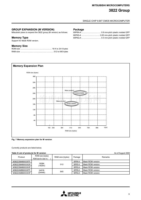
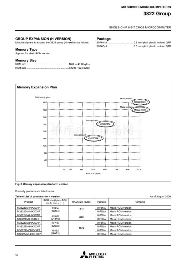
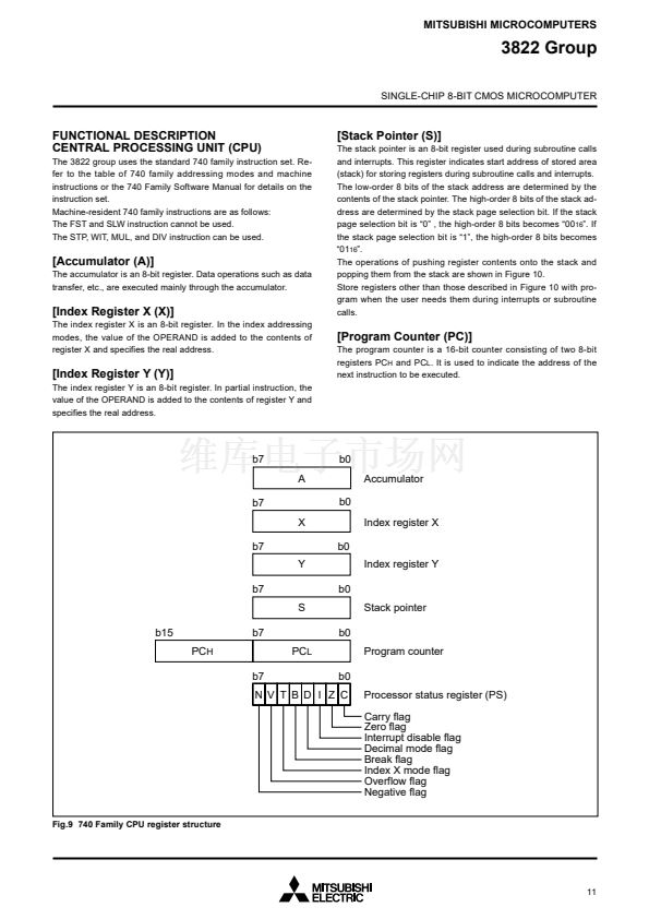
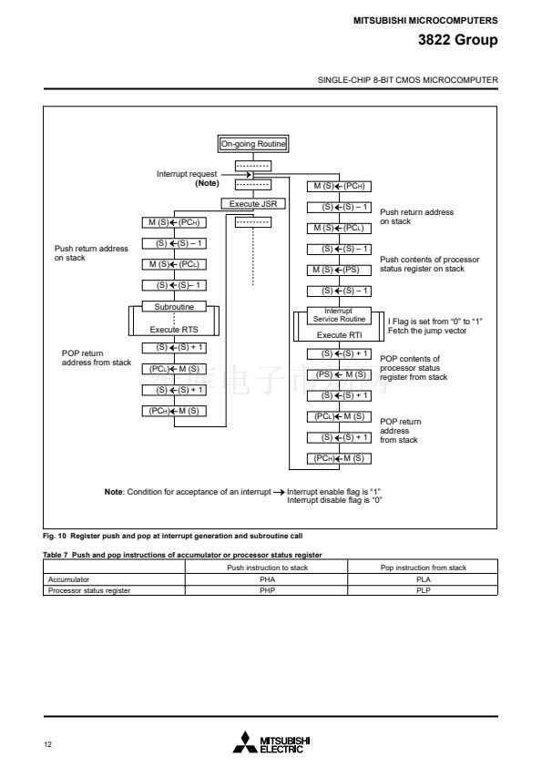
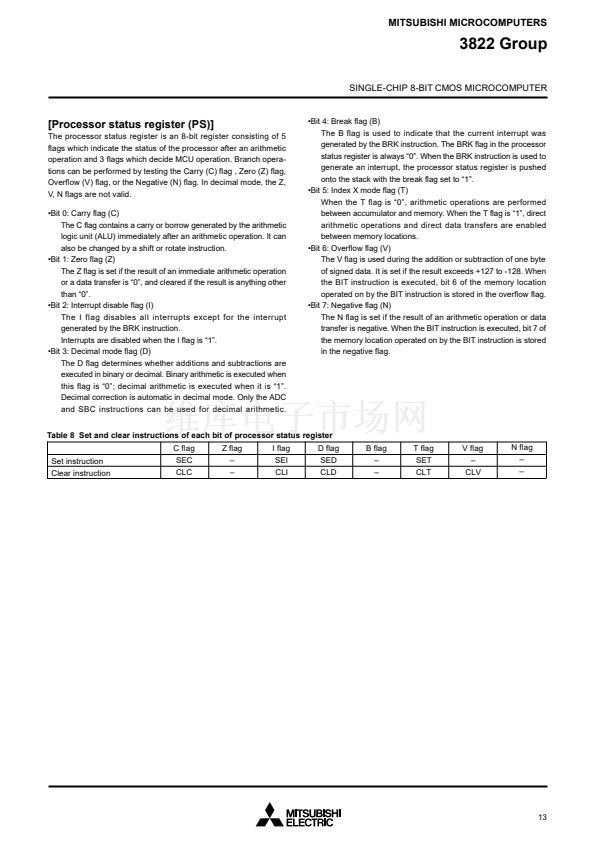
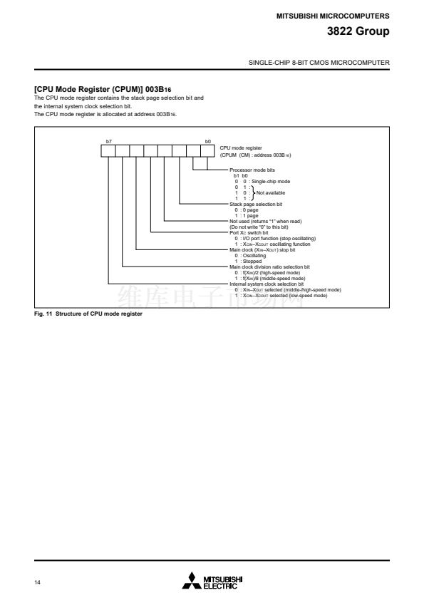
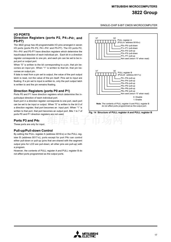
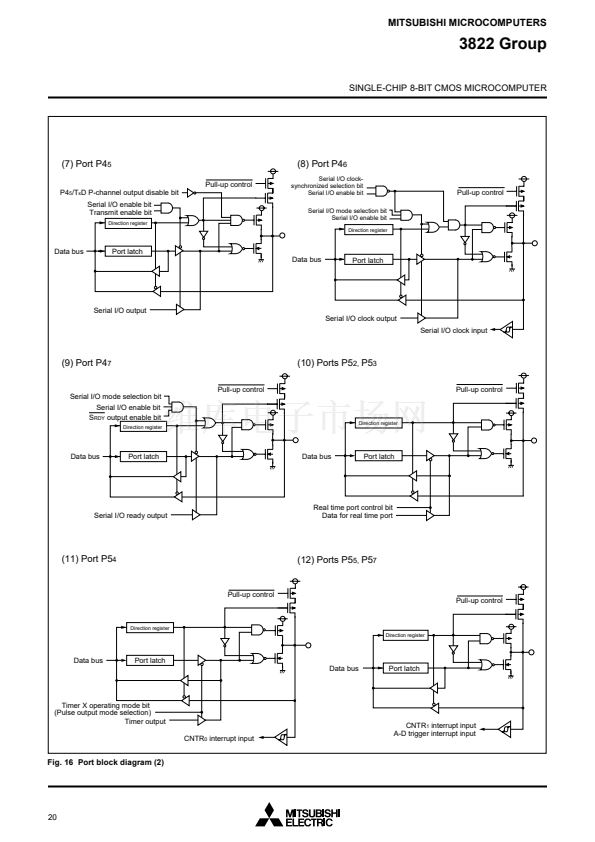
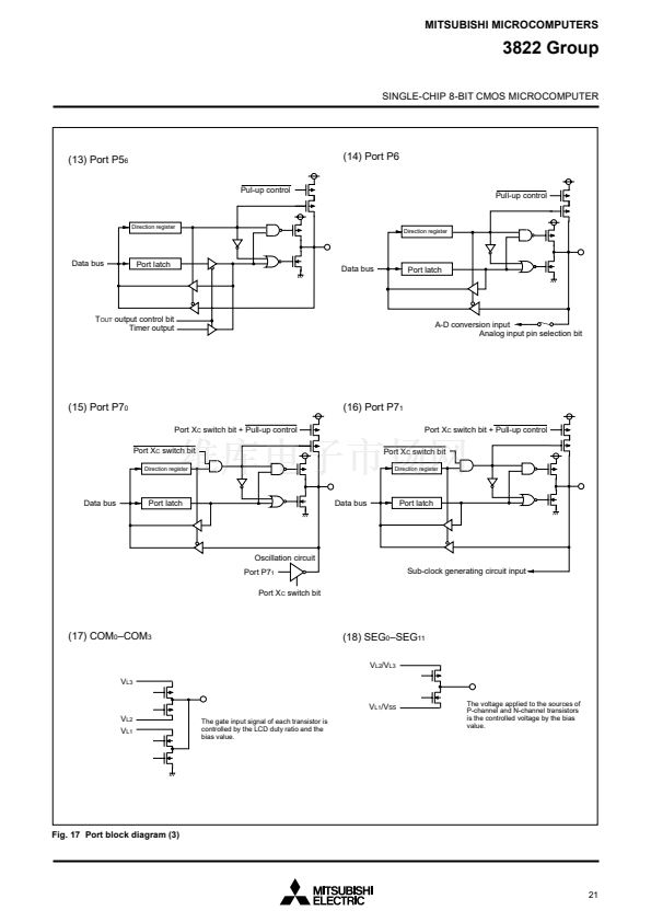
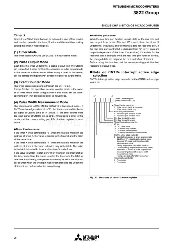
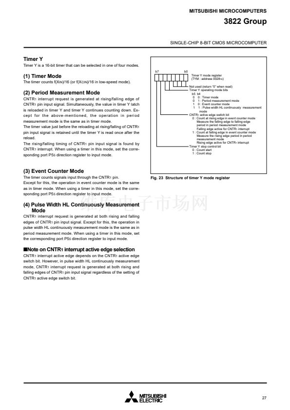
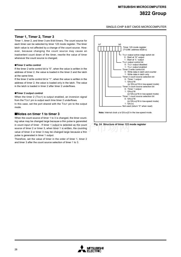
MITSUBISHI MICROCOMPUTERS
3822 Group
SINGLE-CHIP 8-BIT CMOS MICROCOMPUTER
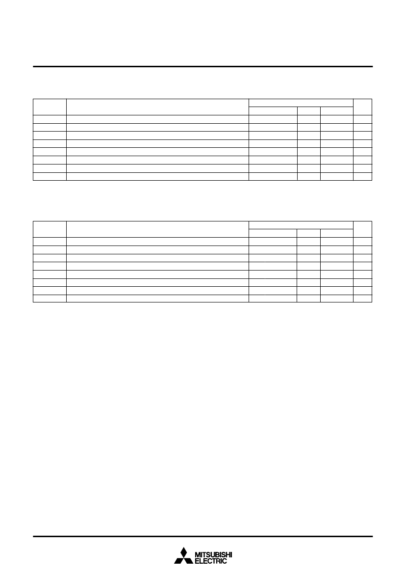
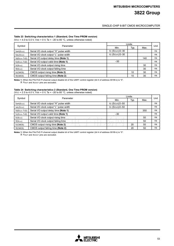
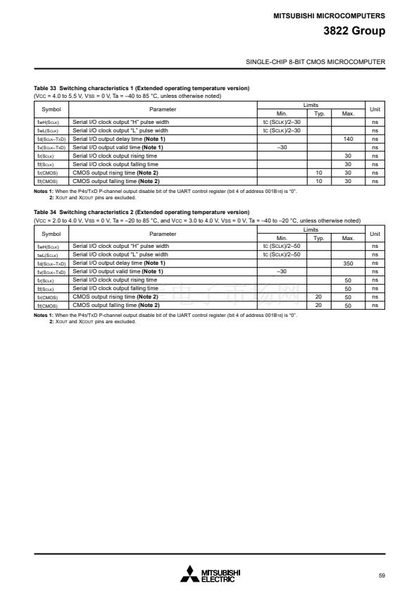
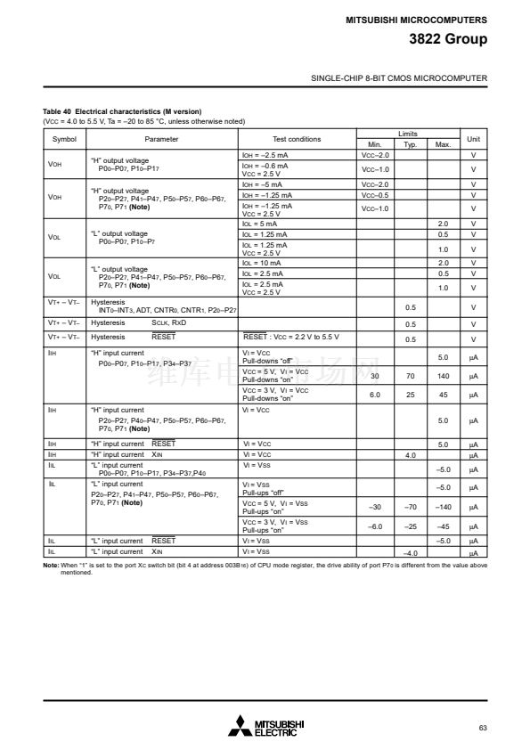
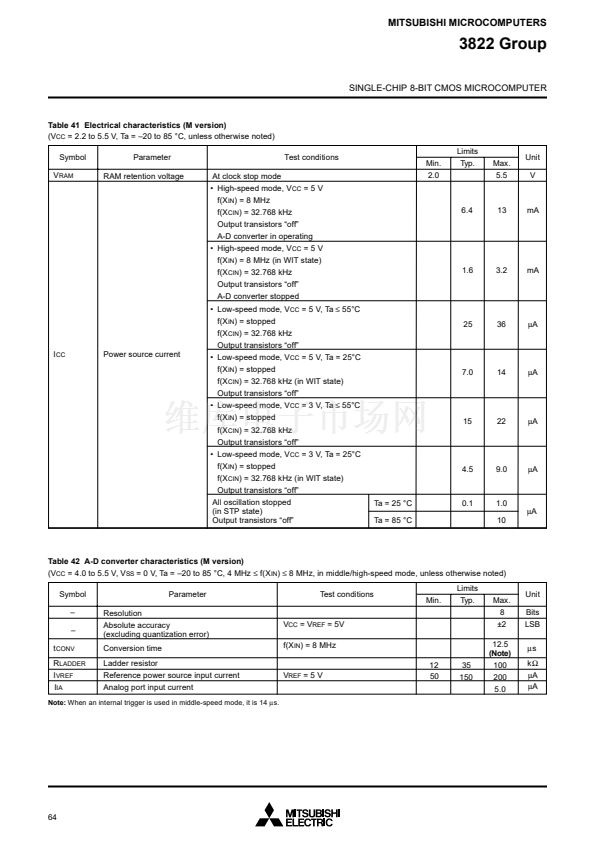
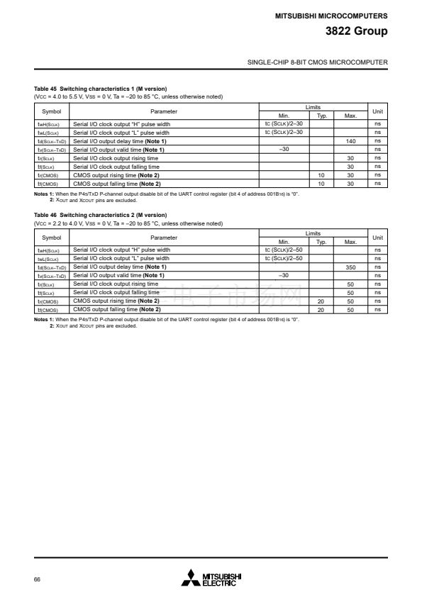
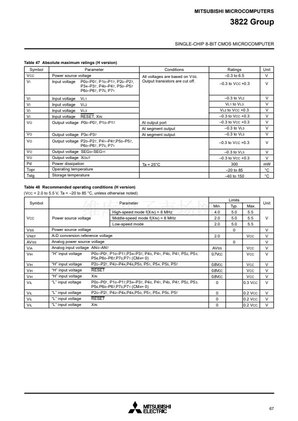
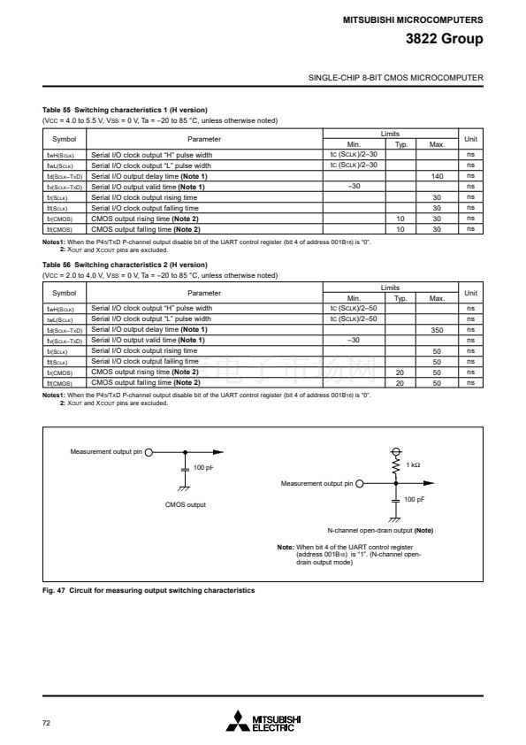
Table 23 Switching characteristics 1 (Standard, One Time PROM version)
(V
CC
= 4.0 to 5.5 V, V
SS
= 0 V, Ta = 鈥?0 to 85 掳C, unless otherwise noted)
Symbol
t
wH(S
CLK
)
t
wL(S
CLK
)
t
d(S
CLK
鈥揟
X
D)
t
v(S
CLK
鈥揟
X
D)
t
r(S
CLK
)
t
f(S
CLK
)
t
r(CMOS)
t
f(CMOS)
Parameter
Serial I/O clock output 鈥淗鈥?pulse width
Serial I/O clock output 鈥淟鈥?pulse width
Serial I/O output delay time
(Note 1)
Serial I/O output valid time
(Note 1)
Serial I/O clock output rising time
Serial I/O clock output falling time
CMOS output rising time
(Note 2)
CMOS output falling time
(Note 2)
Limits
Min.
t
C
(S
CLK
)/2鈥?0
t
C
(S
CLK
)/2鈥?0
鈥?0
30
10
10
30
30
30
Typ.
Max.
Unit
ns
ns
140
ns
ns
ns
ns
ns
ns
Notes 1:
When the P4
5
/T
X
D P-channel output disable bit of the UART control register (bit 4 of address 001B
16
) is 鈥?鈥?
2:
X
OUT
and X
COUT
pins are excluded.
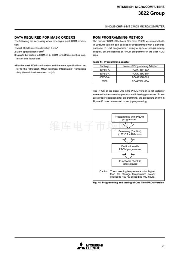
Table 24 Switching characteristics 2 (Standard, One Time PROM version)
(V
CC
= 2.5 to 4.0 V, V
SS
= 0 V, Ta = 鈥?0 to 85 掳C, unless otherwise noted)
Symbol
t
wH(S
CLK
)
twL(S
CLK
)
Parameter
Serial I/O clock output 鈥淗鈥?pulse width
Serial I/O clock output 鈥淟鈥?pulse width
Serial I/O output delay time
(Note 1)
Serial I/O output valid time
(Note 1)
Serial I/O clock output rising time
Serial I/O clock output falling time
CMOS output rising time
(Note 2)
CMOS output falling time
(Note 2)
Limits
Min.
t
C
(S
CLK
)/2鈥?0
t
C
(S
CLK
)/2鈥?0
鈥?0
50
20
20
50
50
50
Typ.
Max.
Unit
ns
t
d(S
CLK
鈥揟
X
D)
t
v(S
CLK
鈥揟
X
D)
t
r(S
CLK
)
t
f(S
CLK
)
t
r(CMOS)
t
f(CMOS)
350
ns
ns
ns
ns
ns
ns
ns
Notes 1:
When the P4
5
/T
X
D P-channel output disable bit of the UART control register (bit 4 of address 001B
16
) is 鈥?鈥?
2:
X
OUT
and X
COUT
pins are excluded.
53


 1
1
 2
2
 3
3
 4
4
 5
5
 6
6
 7
7
 8
8
 9
9
 10
10
 11
11
 12
12
 13
13
 14
14
 15
15
 16
16
 17
17
 18
18
 19
19
 20
20
 21
21
 22
22
 23
23
 24
24
 25
25
 26
26
 27
27
 28
28
 29
29
 30
30
 31
31
 32
32
 33
33
 34
34
 35
35
 36
36
 37
37
 38
38
 39
39
 40
40
 41
41
 42
42
 43
43
 44
44
 45
45
 46
46
 47
47
 48
48
 49
49
 50
50
 51
51
 52
52
 53
53
 54
54
 55
55
 56
56
 57
57
 58
58
 59
59
 60
60
 61
61
 62
62
 63
63
 64
64
 65
65
 66
66
 67
67
 68
68
 69
69
 70
70
 71
71
 72
72
 73
73
 74
74
 75
75
 76
76
 77
77
 78
78
