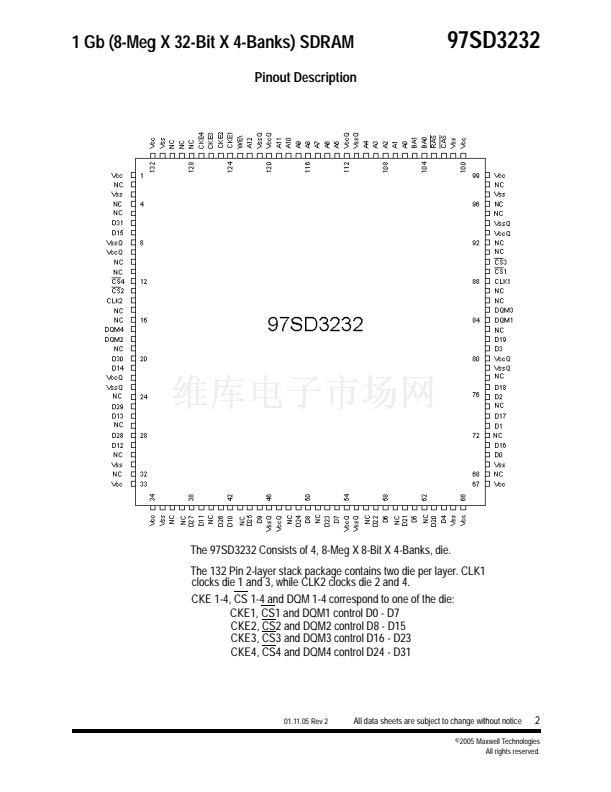
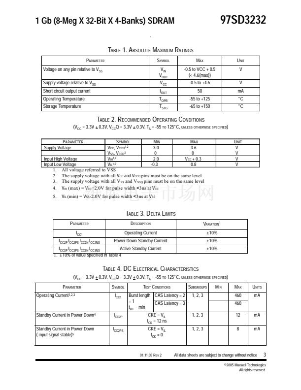
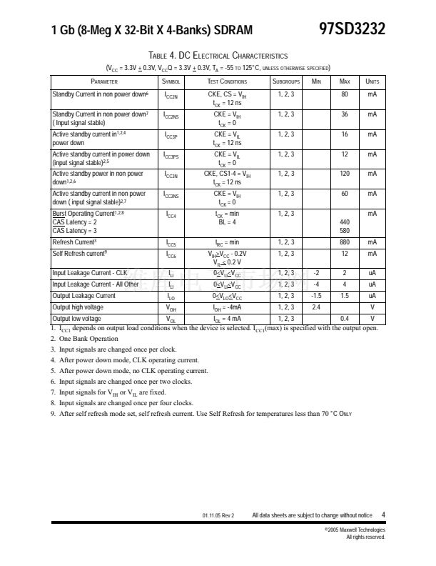
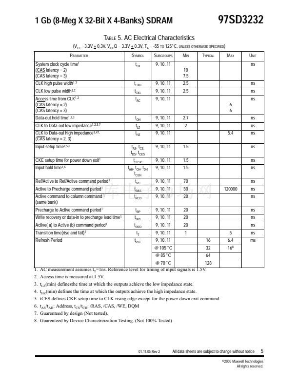
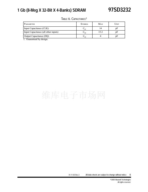
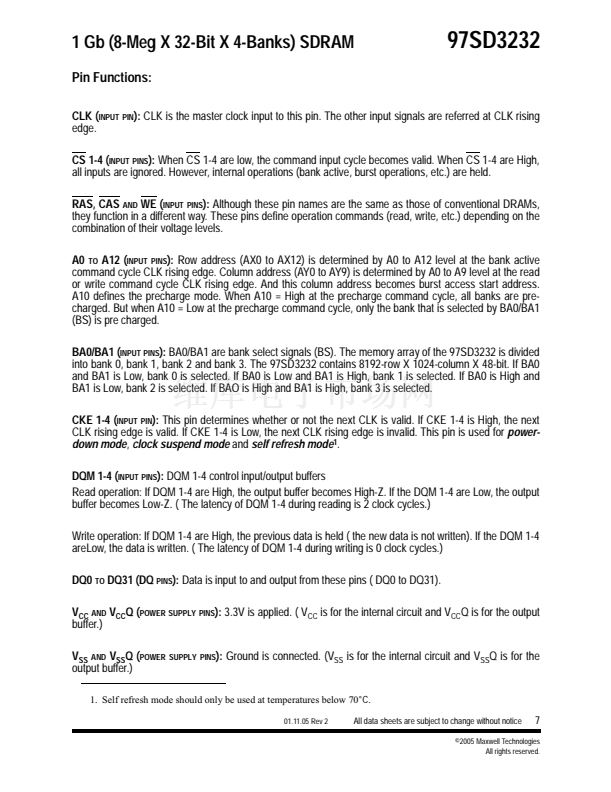
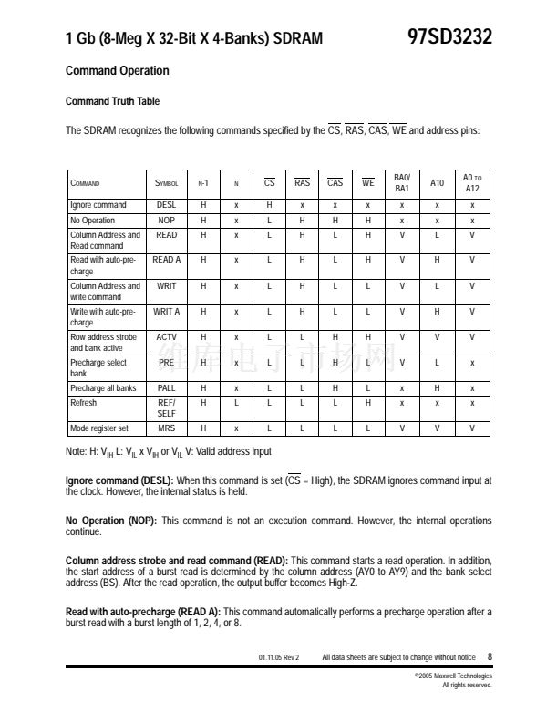
1 Gb (8-Meg X 32-Bit X 4-Banks) SDRAM
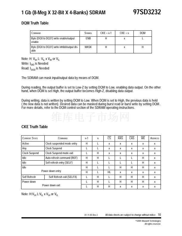
DQM Truth Table
C
OMMAND
Byte (DQ0 to DQ31) write enable/output
enable
Byte (DQ0 to DQ31) write inhibit/output dis-
able
S
YMBOL
ENB
MASK
CKE =
N
-1
H
H
CKE =
N
x
x
97SD3232
DQM
L
H
Note: H: V
IH
L: V
IL
x V
IH
or V
IL
Write: I
DID
is Needed
Read: I
DOD
is Needed
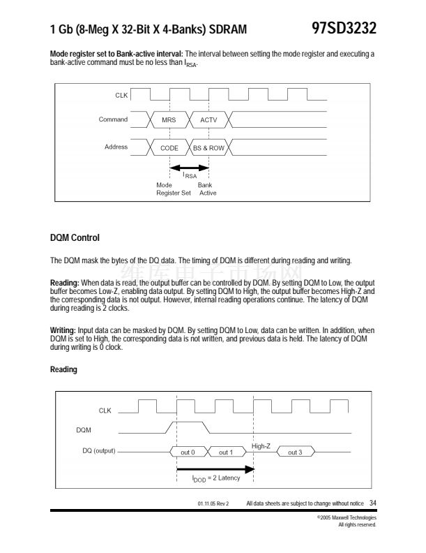
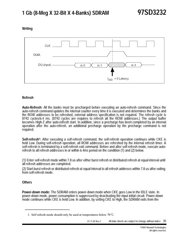
The SDRAM can mask input/output data by means of DQM.
During reading, the output buffer is set to Low-Z by setting DQM to Low, enabling data output. On the other
hand, when DQM is set High, the output buffer becomes High-Z, disabling data output.
Memory
During writing, data is written by setting DQM to Low. When DQM is set to High, the previous data is held
( the new data is not written). Desired data can be masked during burst read or burst write by setting DQM..
For more details, refer to the DQM control section of the SDRAM operating instructions.
CKE Truth Table
C
URRENT
S
TATE
Active
Any
Clock Suspend
Idle
Idle
Idle
Power down entry
Self Refresh
Power down
Power down exit
Self Refresh exit (SELFX)
C
OMMAND
Clock suspended mode entry
Clock Suspend
Clock Suspend mode exit
Auto-refresh command (REF)
Self-refresh entry (SELF)
N
-1
N
CS
x
x
x
L
L
L
HL
L
L
H
RAS
x
x
x
L
L
H
x
H
H
x
CAS
x
x
x
L
L
H
x
H
H
x
WE
x
x
x
H
H
H
x
H
H
x
A
DDRESS
x
x
x
x
x
x
x
x
x
x
H
L
L
H
H
H
H
L
L
L
L
L
H
H
L
L
L
H
H
H
Note: H:V
IH
L:V
IL
x V
IH
or V
IL
01.11.05 Rev 2
All data sheets are subject to change without notice
10
漏2005 Maxwell Technologies
All rights reserved.


 1
1
 2
2
 3
3
 4
4
 5
5
 6
6
 7
7
 8
8
 9
9
 10
10
 11
11
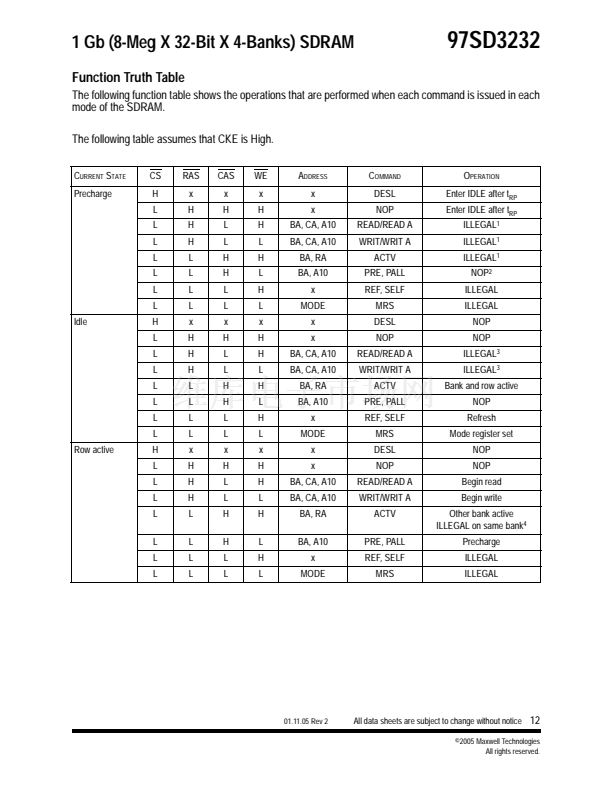 12
12
 13
13
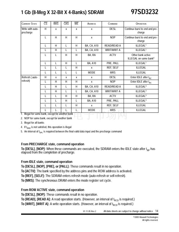 14
14
 15
15
 16
16
 17
17
 18
18
 19
19
 20
20
 21
21
 22
22
 23
23
 24
24
 25
25
 26
26
 27
27
 28
28
 29
29
 30
30
 31
31
 32
32
 33
33
 34
34
 35
35
 36
36
 37
37
 38
38
 39
39
