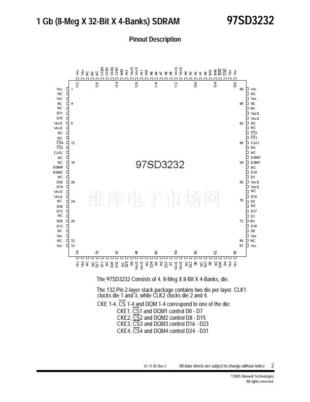
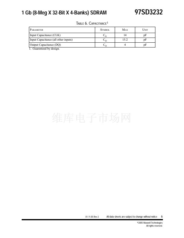
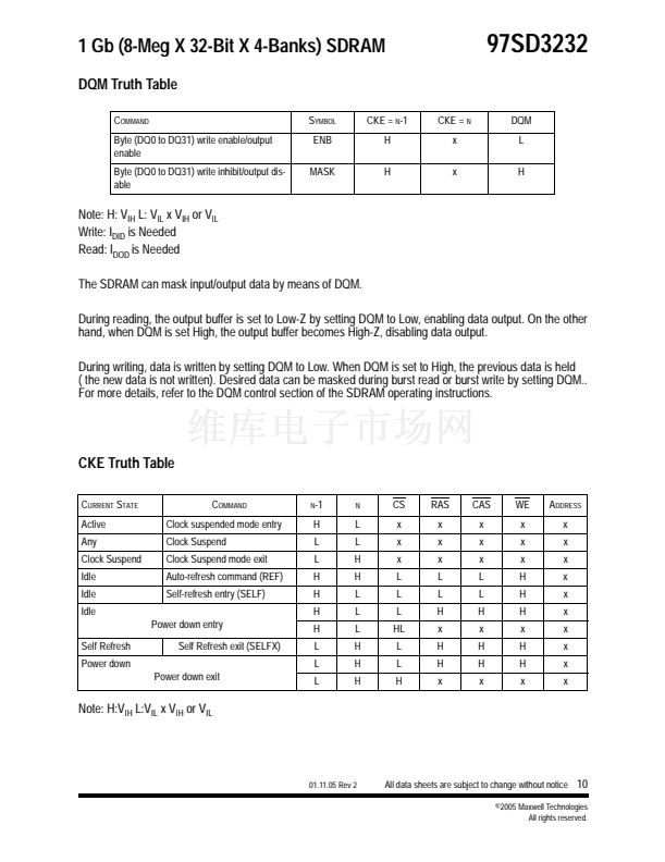
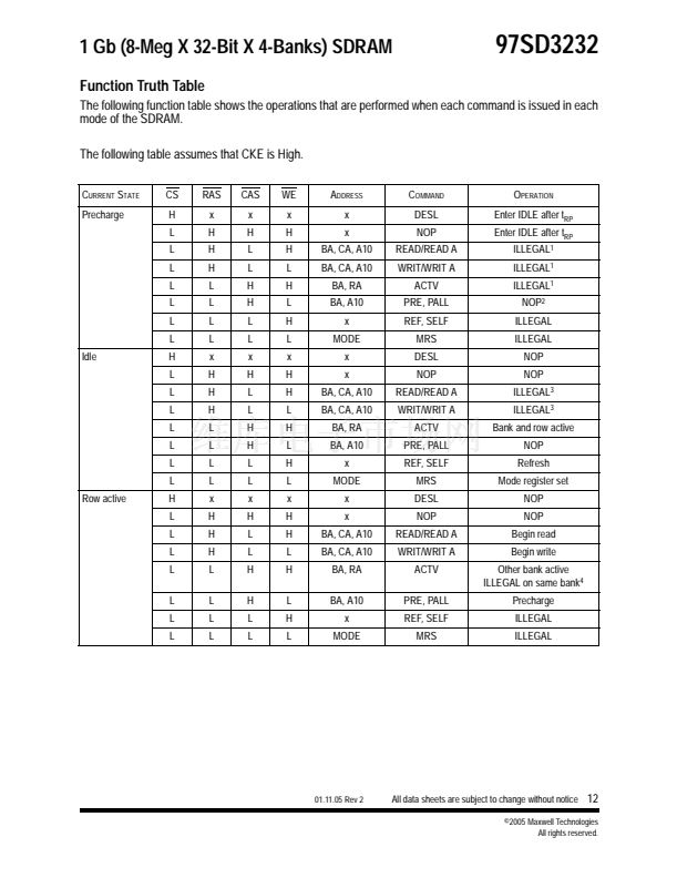
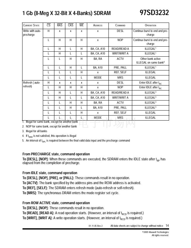
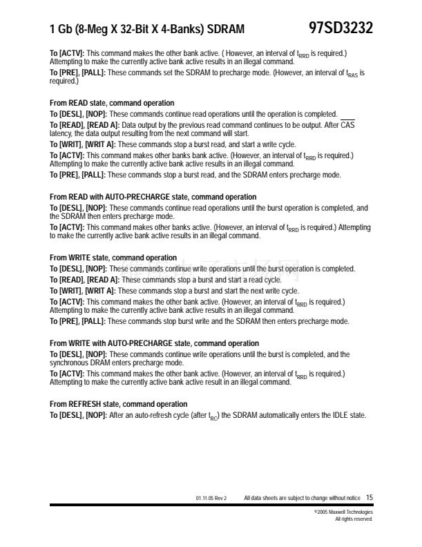
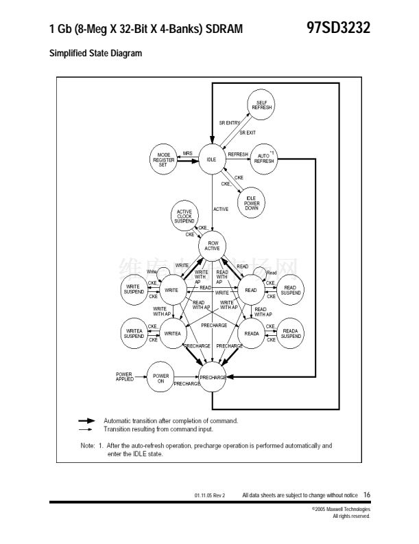
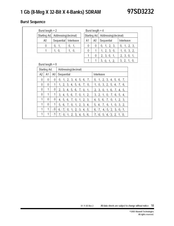
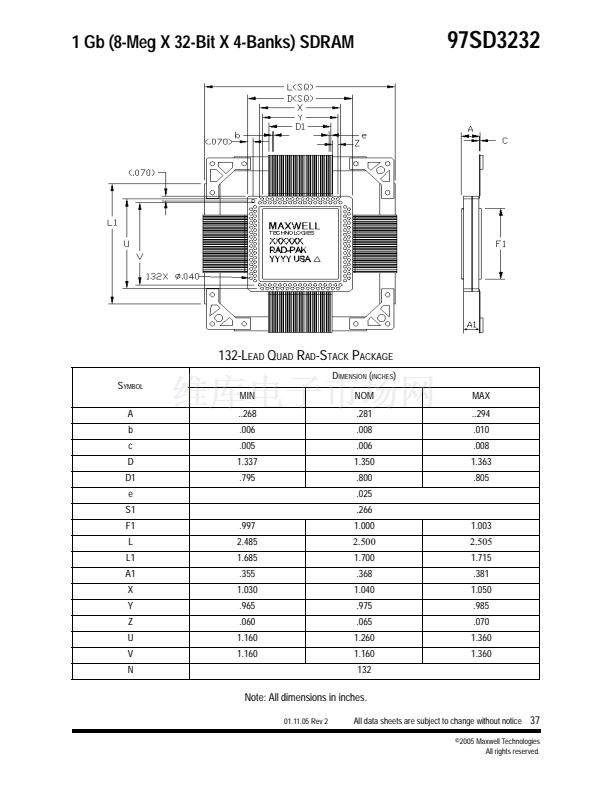
1 Gb (8-Meg X 32-Bit X 4-Banks) SDRAM
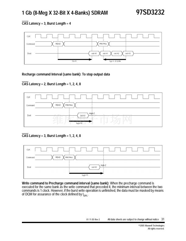
CAS Latency = 3, Burst Length = 4
97SD3232
Recharge command Interval (same bank): To stop output data
CAS Latency = 2, Burst Length = 1, 2, 4, 8
Memory
CAS Latency = 3, Burst Length = 1, 2, 4, 8
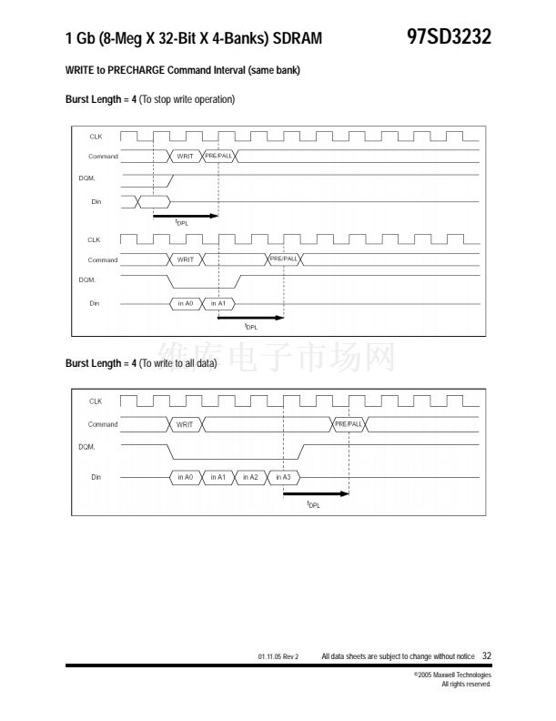
Write command to Precharge command interval (same bank):
When the precharge command is
executed for the same bank as the write command that preceded it, the minimum interval between the two
commands is 1 clock. However, if the burst write operation is unfinished, the data must be masked by means
of DQM for assurance of the clock defined by t
DPL
.
01.11.05 Rev 2
All data sheets are subject to change without notice
31
漏2005 Maxwell Technologies
All rights reserved.


 1
1
 2
2
 3
3
 4
4
 5
5
 6
6
 7
7
 8
8
 9
9
 10
10
 11
11
 12
12
 13
13
 14
14
 15
15
 16
16
 17
17
 18
18
 19
19
 20
20
 21
21
 22
22
 23
23
 24
24
 25
25
 26
26
 27
27
 28
28
 29
29
 30
30
 31
31
 32
32
 33
33
 34
34
 35
35
 36
36
 37
37
 38
38
 39
39
