1 Gb (8-Meg X 32-Bit X 4-Banks) SDRAM
97SD3232
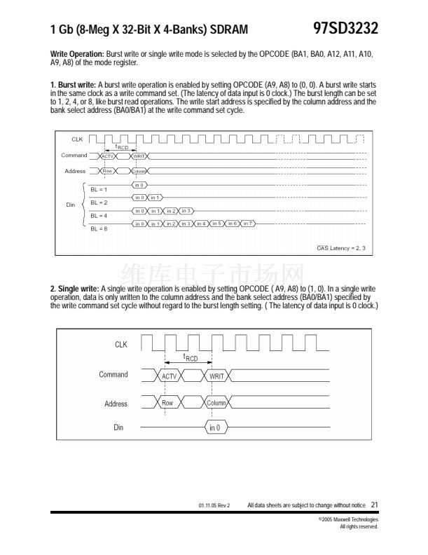
Write Operation:
Burst write or single write mode is selected by the OPCODE (BA1, BA0, A12, A11, A10,
A9, A8) of the mode register.
1. Burst write:
A burst write operation is enabled by setting OPCODE (A9, A8) to (0, 0). A burst write starts
in the same clock as a write command set. (The latency of data input is 0 clock.) The burst length can be set
to 1, 2, 4, or 8, like burst read operations. The write start address is specified by the column address and the
bank select address (BA0/BA1) at the write command set cycle.
Memory
2. Single write:
A single write operation is enabled by setting OPCODE ( A9, A8) to (1, 0). In a single write
operation, data is only written to the column address and the bank select address (BA0/BA1) specified by
the write command set cycle without regard to the burst length setting. ( The latency of data input is 0 clock.)
01.11.05 Rev 2
All data sheets are subject to change without notice
21
漏2005 Maxwell Technologies
All rights reserved.


 1
1
 2
2
 3
3
 4
4
 5
5
 6
6
 7
7
 8
8
 9
9
 10
10
 11
11
 12
12
 13
13
 14
14
 15
15
 16
16
 17
17
 18
18
 19
19
 20
20
 21
21
 22
22
 23
23
 24
24
 25
25
 26
26
 27
27
 28
28
 29
29
 30
30
 31
31
 32
32
 33
33
 34
34
 35
35
 36
36
 37
37
 38
38
 39
39
