1 Gb (8-Meg X 32-Bit X 4-Banks) SDRAM
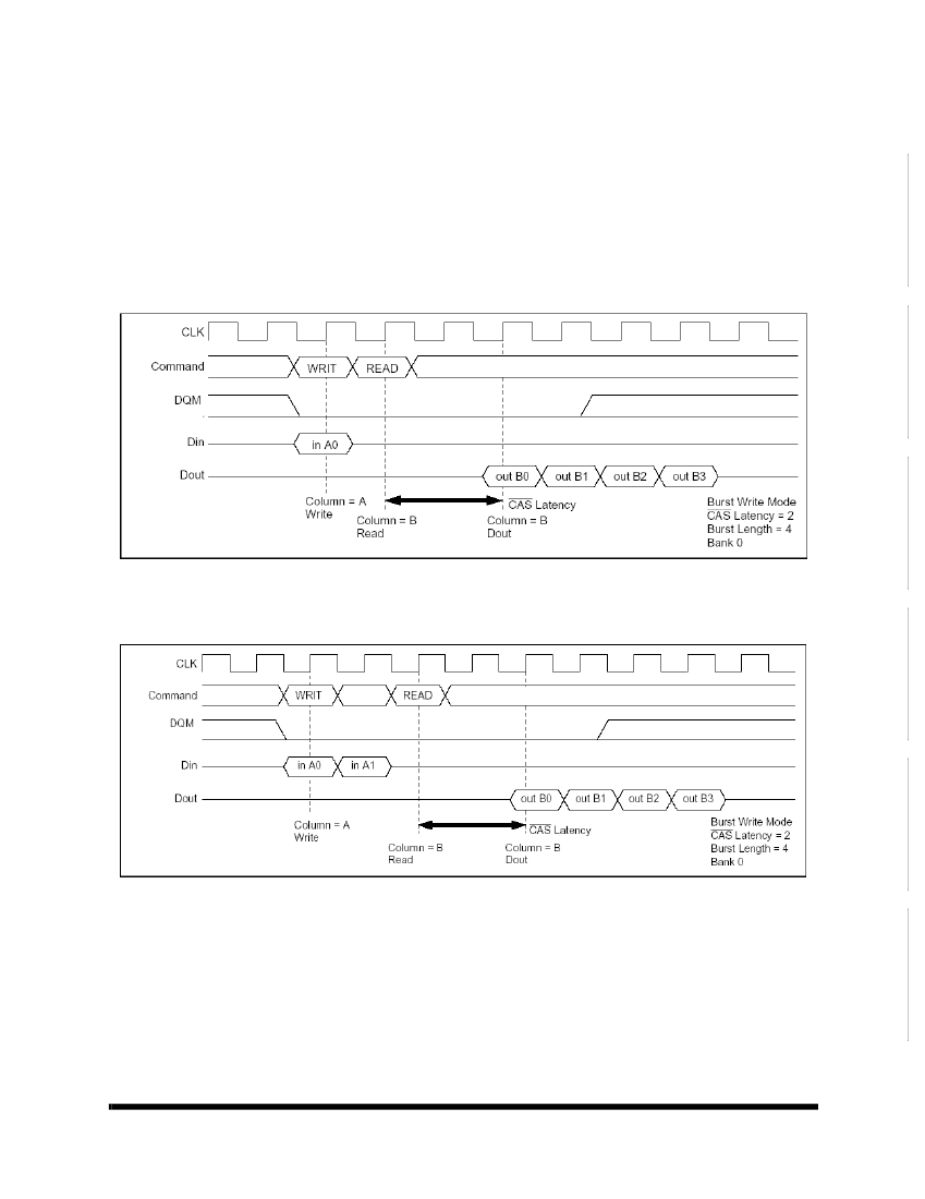
Write command to READ command interval:
97SD3232
1. Same bank, same ROW address:
When the read command is executed at the same ROW address of
the same bank as the preceding write command, the read command can be performed after an interval of no
less than 1 clock. However, in the case of a burst write, data will continue to be written until one clock before
the read command is executed.
WRITE to READ Command Interval (1)
Memory
Write to READ Command Interval (2)
2. Same bank, different ROW address:
When the ROW address changes, consecutive read commands
cannot be executed; it is necessary to separate the two commands with a precharge command and a bank-
active command.
3. Different bank:
When the bank changes, the read command can be performed after an interval of no less
than 1 clock, provided that the other bank is in the bank-active state. However, in the case of a burst write,
data will continue to be written until one clock before the read command is executed (as in the case of the
same bank and the same address).
01.11.05 Rev 2
All data sheets are subject to change without notice
27
漏2005 Maxwell Technologies
All rights reserved.
