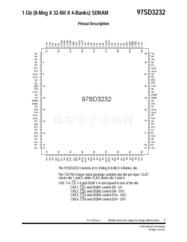
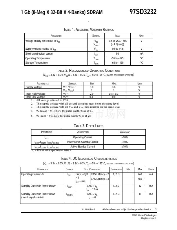
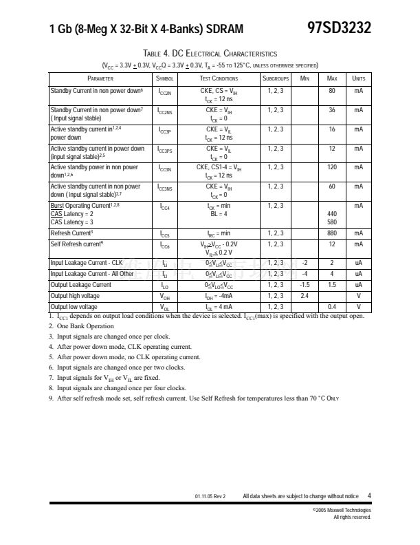
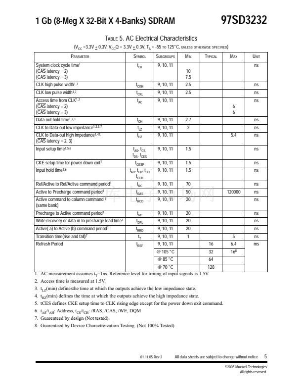
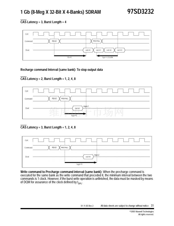
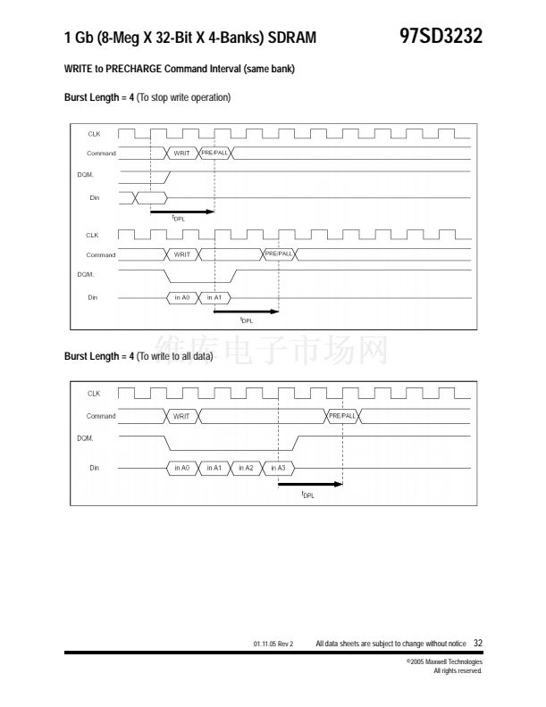
1 Gb (8-Meg X 32-Bit X 4-Banks) SDRAM
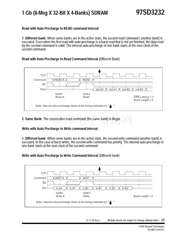
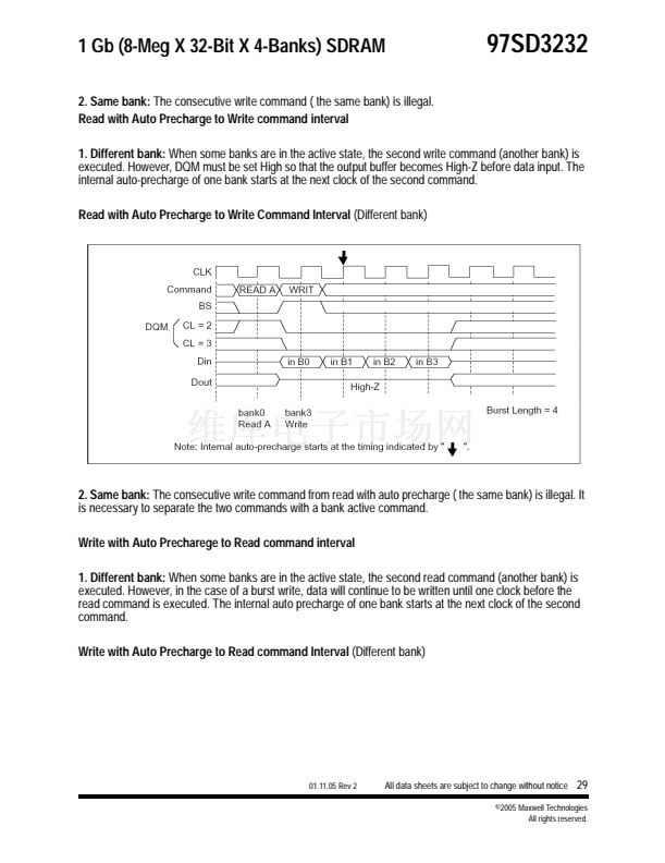
2. Same bank:
The consecutive write command ( the same bank) is illegal.
Read with Auto Precharge to Write command interval
97SD3232
1. Different bank:
When some banks are in the active state, the second write command (another bank) is
executed. However, DQM must be set High so that the output buffer becomes High-Z before data input. The
internal auto-precharge of one bank starts at the next clock of the second command.
Read with Auto Precharge to Write Command Interval
(Different bank)
Memory
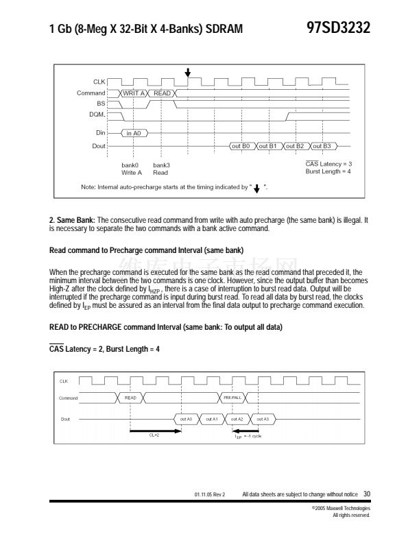
2. Same bank:
The consecutive write command from read with auto precharge ( the same bank) is illegal. It
is necessary to separate the two commands with a bank active command.
Write with Auto Precharege to Read command interval
1. Different bank:
When some banks are in the active state, the second read command (another bank) is
executed. However, in the case of a burst write, data will continue to be written until one clock before the
read command is executed. The internal auto precharge of one bank starts at the next clock of the second
command.
Write with Auto Precharge to Read command Interval
(Different bank)
01.11.05 Rev 2
All data sheets are subject to change without notice
29
漏2005 Maxwell Technologies
All rights reserved.


 1
1
 2
2
 3
3
 4
4
 5
5
 6
6
 7
7
 8
8
 9
9
 10
10
 11
11
 12
12
 13
13
 14
14
 15
15
 16
16
 17
17
 18
18
 19
19
 20
20
 21
21
 22
22
 23
23
 24
24
 25
25
 26
26
 27
27
 28
28
 29
29
 30
30
 31
31
 32
32
 33
33
 34
34
 35
35
 36
36
 37
37
 38
38
 39
39
