1 Gb (8-Meg X 32-Bit X 4-Banks) SDRAM
97SD3232
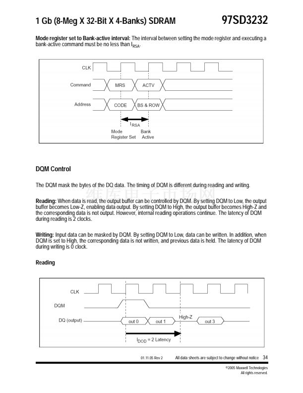
Mode register set to Bank-active interval:
The interval between setting the mode register and executing a
bank-active command must be no less than I
RSA
.
Memory
DQM Control
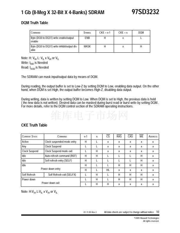
The DQM mask the bytes of the DQ data. The timing of DQM is different during reading and writing.
Reading:
When data is read, the output buffer can be controlled by DQM. By setting DQM to Low, the output
buffer becomes Low-Z, enabling data output. By setting DQM to High, the output buffer becomes High-Z and
the corresponding data is not output. However, internal reading operations continue. The latency of DQM
during reading is 2 clocks.
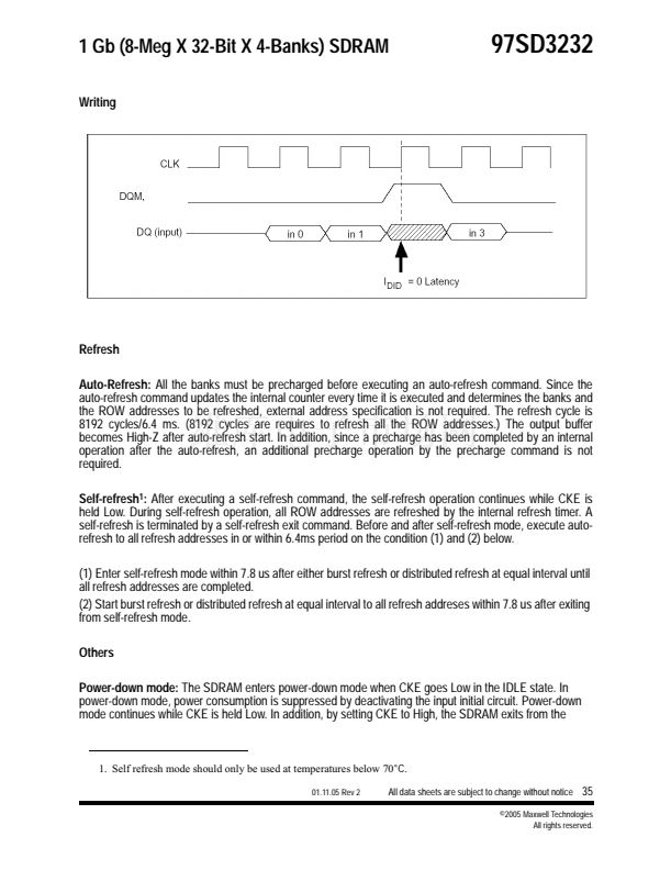
Writing:
Input data can be masked by DQM. By setting DQM to Low, data can be written. In addition, when
DQM is set to High, the corresponding data is not written, and previous data is held. The latency of DQM
during writing is 0 clock.
Reading
01.11.05 Rev 2
All data sheets are subject to change without notice
34
漏2005 Maxwell Technologies
All rights reserved.


 1
1
 2
2
 3
3
 4
4
 5
5
 6
6
 7
7
 8
8
 9
9
 10
10
 11
11
 12
12
 13
13
 14
14
 15
15
 16
16
 17
17
 18
18
 19
19
 20
20
 21
21
 22
22
 23
23
 24
24
 25
25
 26
26
 27
27
 28
28
 29
29
 30
30
 31
31
 32
32
 33
33
 34
34
 35
35
 36
36
 37
37
 38
38
 39
39
