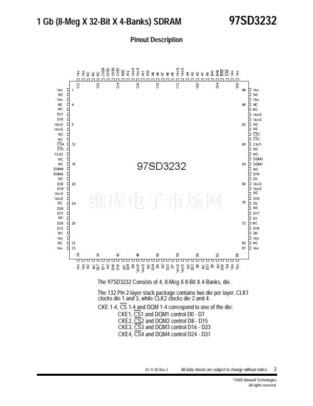
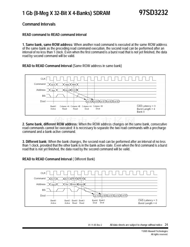
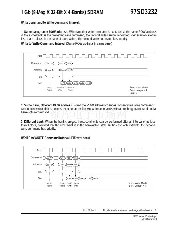
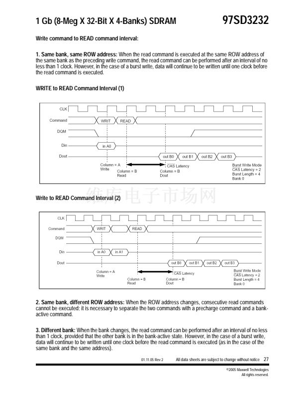
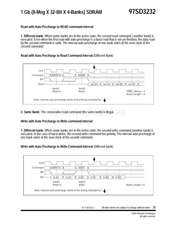
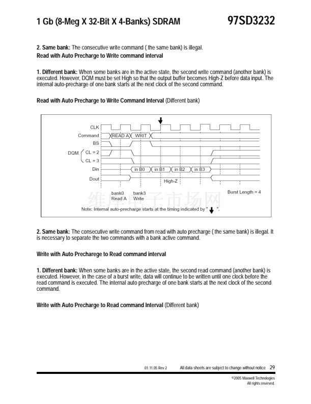
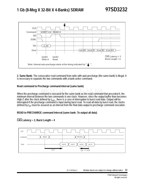
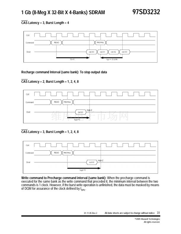
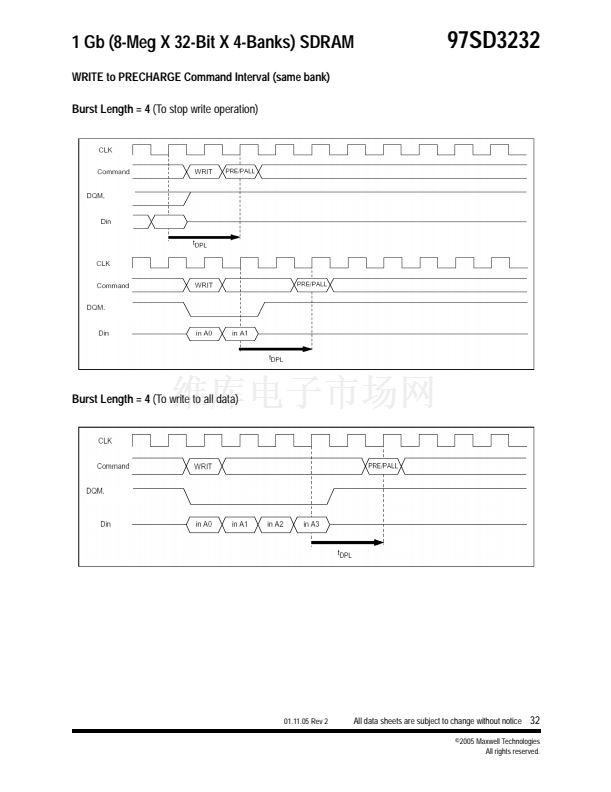
1 Gb (8-Meg X 32-Bit X 4-Banks) SDRAM
Pin Functions:
97SD3232
CLK (
INPUT PIN
):
CLK is the master clock input to this pin. The other input signals are referred at CLK rising
edge.
CS 1-4 (
INPUT PINS
):
When CS 1-4 are low, the command input cycle becomes valid. When CS 1-4 are High,
all inputs are ignored. However, internal operations (bank active, burst operations, etc.) are held.
RAS, CAS
AND
WE (
INPUT PINS
):
Although these pin names are the same as those of conventional DRAMs,
they function in a different way. These pins define operation commands (read, write, etc.) depending on the
combination of their voltage levels.
A0
TO
A12 (
INPUT PINS
):
Row address (AX0 to AX12) is determined by A0 to A12 level at the bank active
command cycle CLK rising edge. Column address (AY0 to AY9) is determined by A0 to A9 level at the read
or write command cycle CLK rising edge. And this column address becomes burst access start address.
A10 defines the precharge mode. When A10 = High at the precharge command cycle, all banks are pre-
charged. But when A10 = Low at the precharge command cycle, only the bank that is selected by BA0/BA1
(BS) is pre charged.
BA0/BA1 (
INPUT PINS
):
BA0/BA1 are bank select signals (BS). The memory array of the 97SD3232 is divided
into bank 0, bank 1, bank 2 and bank 3. The 97SD3232 contains 8192-row X 1024-column X 48-bit. If BA0
and BA1 is Low, bank 0 is selected. If BA0 is Low and BA1 is High, bank 1 is selected. If BA0 is High and
BA1 is Low, bank 2 is selected. If BAO is High and BA1 is High, bank 3 is selected.
CKE 1-4 (
INPUT PIN
):
This pin determines whether or not the next CLK is valid. If CKE 1-4 is High, the next
CLK rising edge is valid. If CKE 1-4 is Low, the next CLK rising edge is invalid. This pin is used for
power-
down mode, clock suspend mode
and
self refresh mode
1
.
DQM 1-4 (
INPUT PINS
):
DQM 1-4 control input/output buffers
Read operation: If DQM 1-4 are High, the output buffer becomes High-Z. If the DQM 1-4 are Low, the output
buffer becomes Low-Z. ( The latency of DQM 1-4 during reading is 2 clock cycles.)
Write operation: If DQM 1-4 are High, the previous data is held ( the new data is not written). If the DQM 1-4
areLow, the data is written. ( The latency of DQM 1-4 during writing is 0 clock cycles.)
DQ0
TO
DQ31 (DQ
PINS
):
Data is input to and output from these pins ( DQ0 to DQ31).
V
CC AND
V
CC
Q (
POWER SUPPLY PINS
):
3.3V is applied. ( V
CC
is for the internal circuit and V
CC
Q is for the output
buffer.)
V
SS AND
V
SS
Q (
POWER SUPPLY PINS
):
Ground is connected. (V
SS
is for the internal circuit and V
SS
Q is for the
output buffer.)
1. Self refresh mode should only be used at temperatures below 70掳C.
01.11.05 Rev 2
Memory
All data sheets are subject to change without notice
7
漏2005 Maxwell Technologies
All rights reserved.


 1
1
 2
2
 3
3
 4
4
 5
5
 6
6
 7
7
 8
8
 9
9
 10
10
 11
11
 12
12
 13
13
 14
14
 15
15
 16
16
 17
17
 18
18
 19
19
 20
20
 21
21
 22
22
 23
23
 24
24
 25
25
 26
26
 27
27
 28
28
 29
29
 30
30
 31
31
 32
32
 33
33
 34
34
 35
35
 36
36
 37
37
 38
38
 39
39
