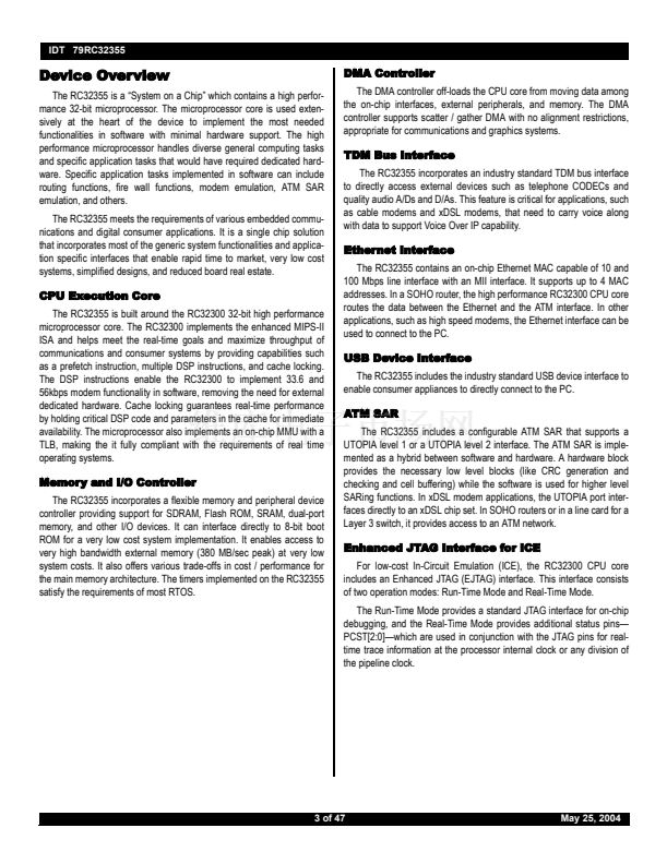
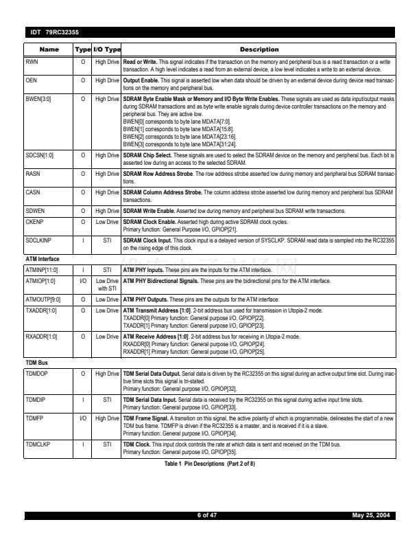
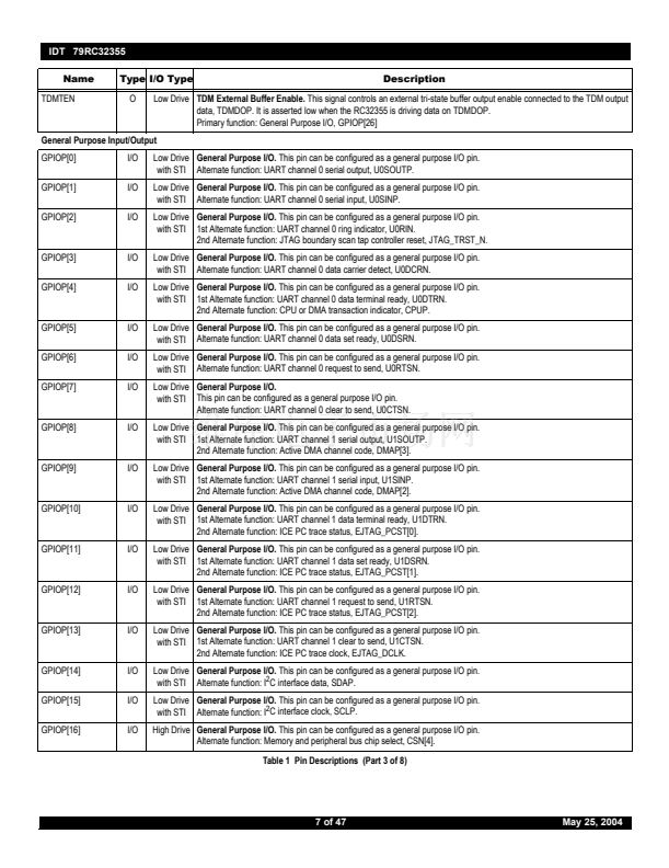
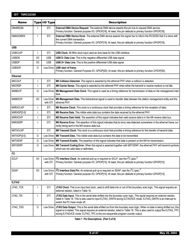
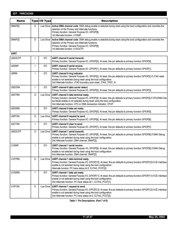
IDT 79RC32355
Pin Description Table
The following table lists the functions of the pins provided on the RC32355. Some of the functions listed may be multiplexed onto the same pin.
To define the active polarity of a signal, a suffix will be used. Signals ending with an 鈥淣鈥?should be interpreted as being active, or asserted, when at
a logic zero (low) level. All other signals (including clocks, buses and select lines) will be interpreted as being active, or asserted when at a logic one
(high) level.
Note:
The input pads of the RC32355 do not contain internal pull-ups or pull-downs. Unused inputs should be tied off to appropriate levels.
This is especially critical for unused control signal inputs (such as BRN) which, if left floating, could adversely affect the RC32355鈥檚 opera-
tion. Also, any input pin left floating can cause a slight increase in power consumption.
Name
System
CLKP
COLDRSTN
RSTN
I
I
I/O
Input
STI
1
System Clock input.
This is the system master clock input. The RISCore 32300 pipeline frequency is a multiple (x2, x3, or
x4) of this clock frequency. All other logic runs at this frequency or less.
Cold Reset.
The assertion of this signal low initiates a cold reset. This causes the RC32355 state to be initialized, boot
configuration to be loaded, and the internal processor PLL to lock onto the system clock (CLKP).
Type I/O Type
Description
Low Drive
Reset.
This bidirectional signal is either driven low or tri-stated, an external pull-up is required to supply the high state. The
with STI RC32355 drives RSTN low during a reset (to inform the external system that a reset is taking place) and then tri-states it.
The external system can drive RSTN low to initiate a warm reset, and then should tri-state it.
High Drive
System clock output.
This is a buffered and delayed version of the system clock input (CLKP). All SDRAM transactions
are synchronous to this clock. This pin should be externally connected to the SDRAMs and to the RC32355 SDCLKINP pin
(SDRAM clock input).
[21:0] High
Memory Address Bus.
26-bit address bus for memory and peripheral accesses. MADDR[20:17] are used for the
Drive
SODIMM data mask enables if SODIMM mode is selected.
[25:22] Low MADDR[22] Primary function: General Purpose I/O, GPIOP[27].
Drive with MADDR[23] Primary function: General Purpose I/O, GPIOP[28].
STI
MADDR[24] Primary function: General Purpose I/O, GPIOP[29].
MADDR[25] Primary function: General Purpose I/O, GPIOP[30].
SYSCLKP
O
Memory and Peripheral Bus
MADDR[25:0]
O
MDATA[31:0]
BDIRN
BOEN[1:0]
I/O
O
O
High Drive
Memory Data Bus.
32-bit data bus for memory and peripheral accesses.
High Drive
External Buffer Direction.
External transceiver direction control for the memory and peripheral data bus, MDATA[31:0]. It
is asserted low during any read transaction, and remains high during write transactions.
High Drive
External Buffer Output Enable.
These signals provide two output enable controls for external data bus transceivers on
the memory and peripheral data bus, MDATA. BOEN[0] is asserted low during external device read transactions. BOEN[1]
is asserted low during SDRAM read transactions.
STI
External Bus Request.
This signal is asserted low by an external master device to request ownership of the memory and
peripheral bus.
BRN
BGN
WAITACKN
I
O
I
Low Drive
External Bus Grant.
This signal is asserted low by RC32355 to indicate that RC32355 has relinquished ownership of the
local memory and peripheral bus to an external master.
STI
Wait or Transfer Acknowledge.
When configured as wait, this signal is asserted low during a memory and peripheral
device bus transaction to extend the bus cycle. When configured as transfer acknowledge, this signal is asserted low dur-
ing a memory and peripheral device bus transaction to signal the completion of the transaction.
CSN[5:0]
O
[3:0]
Device Chip Select.
These signals are used to select an external device on the memory and peripheral bus during device
High Drive transactions. Each bit is asserted low during an access to the selected external device.
CSN[4] Primary function: General purpose I/O, GPIOP[16].
[5:4]
CSN[5] Primary function: General purpose I/O, GPIOP[17].
Low Drive
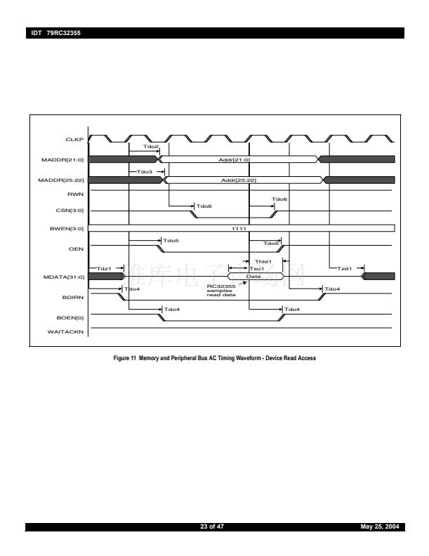
Table 1 Pin Descriptions (Part 1 of 8)
5 of 47
May 25, 2004


 1
1
 2
2
 3
3
 4
4
 5
5
 6
6
 7
7
 8
8
 9
9
 10
10
 11
11
 12
12
 13
13
 14
14
 15
15
 16
16
 17
17
 18
18
 19
19
 20
20
 21
21
 22
22
 23
23
 24
24
 25
25
 26
26
 27
27
 28
28
 29
29
 30
30
 31
31
 32
32
 33
33
 34
34
 35
35
 36
36
 37
37
 38
38
 39
39
 40
40
 41
41
 42
42
 43
43
 44
44
 45
45
 46
46
 47
47
