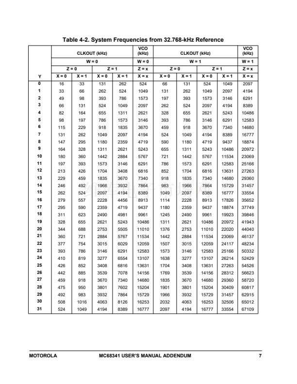
A VCO overshoot can occur when increasing the operating frequency by changing the Y bits in the SYNCR
register. The effects of this overshoot can be controlled by following this procedure:
1. Write the X bit to zero. This will reduce the previous frequency by one half.
2. Write the Y bits to the desired frequency divided by 2.
3. After the VCO lock has occurred, write the X bit to one. This changes the
clock frequency to the desired frequency.
Steps 1 and 2 may be combined.
30. RCCR Initialization
Add to the RCCR description on page 4-41: the RCCR register is unaffected by a processor reset, and contains
an arbitrary value on initial powerup of the RTC. Calibration software should clear the RCCR register before
beginning the calibration process, since RTC operation with an invalid RCDx value is undefined. RCCR[7] is
reserved - on current silicon it always reads 0, and should always be written 0.
31. RCCR Typos
On page 4-42, delete the first description for RCD4-RCD0 near the top of the page.
32. MONTH Register Range
The valid range for the MONTH register on page 4-43 is 1-12, with 鈥?鈥?corresponding to January and 鈥?2鈥?cor-
responding to December.
33. SIM41 Example Code
On page 4-49, about mid-page, change 鈥淢OVEQ #8-1,D0鈥?to 鈥淢OVEQ #16-1,D0鈥?to initialize all 8 chip se-
lects.
34. Bus Error Stack Frame
On page 5-61, in the next-to-last paragraph, delete 鈥?the internal transfer count register is located at SP+$10
and the SSW is located at SP+12)鈥? The stack space allocation is the same for both faults - the location of the
internal count register and SSW remains the same. The only difference is that the faulted instruction program
counter location SP+10 and SP+12 will contain invalid data. To tell the difference between the two stack
frames, look at the first nibble of the faulted exception format vector word located at SP+$E - it will be $0 for
the four-word frame, and $2 for the six-word frame.
35. DSO Timing
On page 5-71, Figure 5-23, DSO transitions one clock later than shown.
36. Typo on BDM RSREG Command
On page 5-77, Section 5.6.2.8.6, RSREG register bit #8 should be a 鈥?鈥?
37. IPIPE Timing
On page 5-88, Figure 5-29 shows the third IPIPE assertion low lasting for 1.5 CLKs - it actually asserts for an
additional 0.5 CLKs. IPIPE transitions occur after the falling edge of CLKOUT.
MOTOROLA
MC68341 USER鈥橲 MANUAL ADDENDUM
10


 1
1
 2
2
 3
3
 4
4
 5
5
 6
6
 7
7
 8
8
 9
9
 10
10
 11
11
 12
12
 13
13
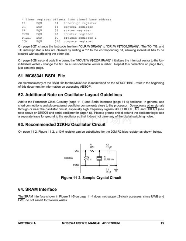
 14
14
 15
15
 16
16
 17
17
 18
18
 19
19
 20
20
 21
21
