scaled by the same factor. This method preserves most of the standard baud rates (19200, 9600, 4800, etc.).
Serial XTAL Frequency
3.6864MHz
1.8432
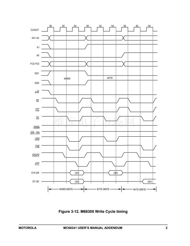
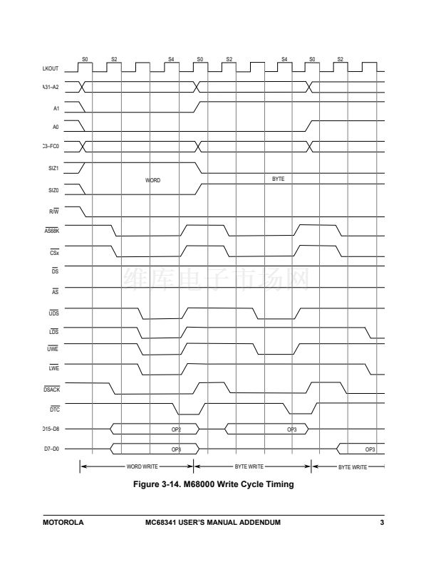
0.9216
CLKOUT Fmin
8.29MHz
4.15
2.07
Max Availabile Baud
Rate
76.8k
38.4k
19.2k
CLKOUT min = 2.25*XTAL frequency
Alternatively, the baud rate clock can be supplied directly through the SCLK input. Since there is a single SCLK
input, both serial channels must use the same baud rate clock, although one could be clocked in the 1x mode
and the other in the 16x mode. When using this method, the X1 input can be tied to ground - no crystal is re-
quired.
56. 68341 Serial Module RTS Difference from 68681
Add to the description for receiver-controlled RTS operation in the next-to-last paragraph on page 7-13: Unlike
the 68681, the RTSx signal does not have to be manually asserted the first time in the mode to support control-
flow capability on the receiver.
57. Additional Note on Serial multidrop operation
Add to the Multidrop Mode section beginning on page 7-15: For multidrop mode, it is not necessary to disable
the transmitter to manipulate the A/D bit, as generally implied in the manual, nor is it necessary to wait until
the previous character completes transmission (i.e. TxEMP). The serial module logic latches this bit and ap-
pends it to the data character when the character is transferred from the transmit buffer to the serial output
shift register. Once this transfer occurs (as indicated by the TxRDY assertion), the A/D bit in MR1 can be
changed without affecting the character in progress. The proper programming sequence to change the A/D
bit for the next character would be:
1.) poll TxRDY until asserted (or interrupt on TxRDY)
2.) set/clear A/D bit in MR1 for new character
3.) write character to transmit buffer (TB)
4.) A/D bit can be changed only after TxRDY asserts again
No other bits in MR1 should be modified when changing the A/D bit.
58. Typo in CPE Description
The CPE bit header on page 8-20 should be "Counter/Prescaler Enable".
59. Typo in Status Register Configuration
On page 8-26, Section 8.5.1, the Status Register (SR) description should say: "鈥?Clear the TO, TG, and TC
bits to reset the interrupts."
60. Typos in Timer Initialization Examples
On pages 8-27 and 8-29, the Timer register offsets should be from the timer base address, not from the SIM41
base address. The correct equates for the Timer register offsets are:
MOTOROLA
MC68341 USER鈥橲 MANUAL ADDENDUM
14


 1
1
 2
2
 3
3
 4
4
 5
5
 6
6
 7
7
 8
8
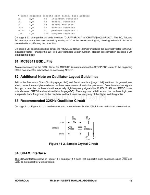
 9
9
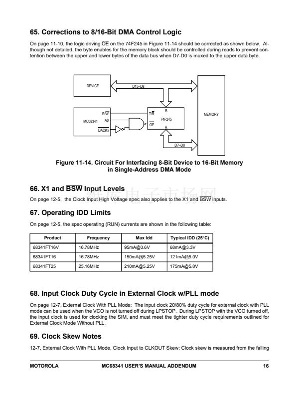
 10
10
 11
11
 12
12
 13
13
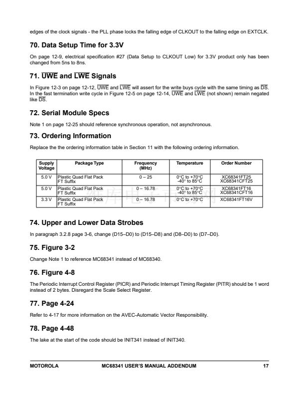
 14
14
 15
15
 16
16
 17
17
 18
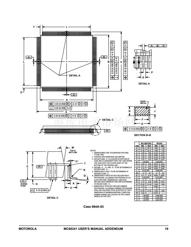
18
 19
19
 20
20
 21
21
