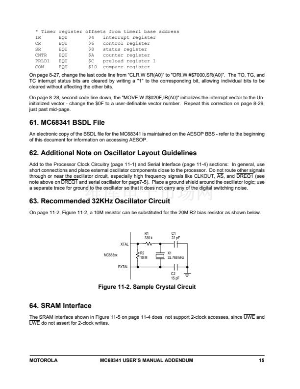
65. Corrections to 8/16-Bit DMA Control Logic
On page 11-10, the logic driving OE on the 74F245 in Figure 11-14 should be corrected as shown below. Al-
though not detailed, the byte enables for the memory block should be controlled during reads to prevent con-
tention between the upper and lower bytes of the data bus when D7-D0 is muxed to the upper data byte.
DEVICE
D15鈥揇8
R/W
MC68341
A0
T/R
OE
B
74F245
A
MEMORY
DACKx
D7鈥揇0
Figure 11-14. Circuit For Interfacing 8-Bit Device to 16-Bit Memory
in Single-Address DMA Mode
66. X1 and BSW Input Levels
On page 12-5, the Clock Input High Voltage spec also applies to the X1 and BSW inputs.
67. Operating IDD Limits
On page 12-5, the spec operating (RUN) currents are shown in the following table:
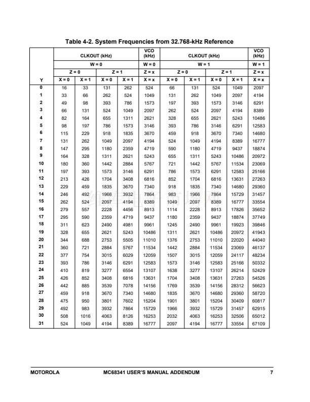
Product
68341FT16V
68341FT16
68341FT25
Frequency
16.78MHz
16.78MHz
25.16MHz
Max Idd
95mA@3.6V
150mA@5.25V
210mA@5.25V
Typical IDD (25掳C)
68mA@3.3V
121mA@5.0V
175mA@5.0V
68. Input Clock Duty Cycle in External Clock w/PLL mode
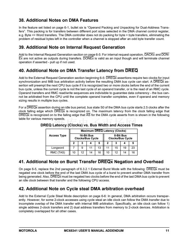
On page 12-7, External Clock With PLL Mode: The input clock 20/80% duty cycle for external clock with PLL
mode can be used when the VCO is not turned off during LPSTOP. During LPSTOP with the VCO turned off,
the input clock is used for clocking the SIM, and must meet the tighter duty cycle requirements outlined for
External Clock Mode Without PLL.
69. Clock Skew Notes
12-7, External Clock With PLL Mode, Clock Input to CLKOUT Skew: Clock skew is measured from the falling
MOTOROLA
MC68341 USER鈥橲 MANUAL ADDENDUM
16


 1
1
 2
2
 3
3
 4
4
 5
5
 6
6
 7
7
 8
8
 9
9
 10
10
 11
11
 12
12
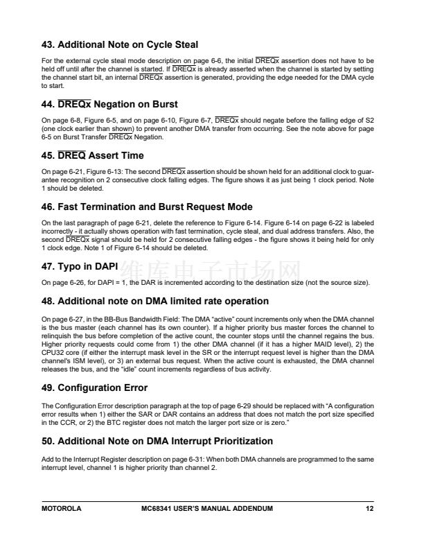 13
13
 14
14
 15
15
 16
16
 17
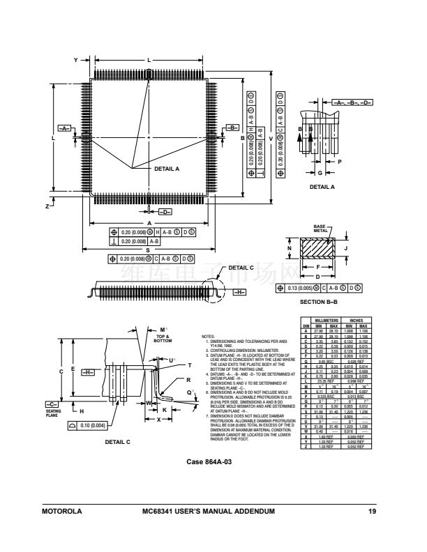
17
 18
18
 19
19
 20
20
 21
21
