See SSTV16856 for driver/buffer version with mode select.
鈥?/div>
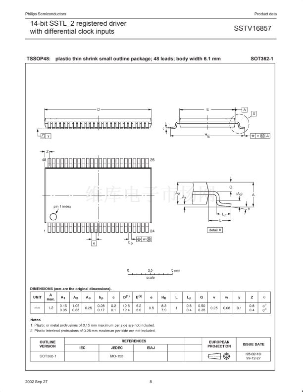
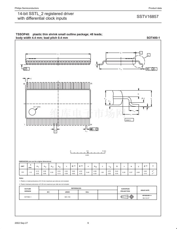
Available in TSSOP-48, TVSOP-48 and 56 ball VFBGA packages
DESCRIPTION
The SSTV16857 is a 14-bit SSTL_2 registered driver with differential
clock inputs, designed to operate between 2.3 V and 2.7 V. V
DDQ
must not exceed V
CC
. Inputs are SSTL_2 type with V
REF
normally at
0.5*V
DDQ
. The outputs support class I which can be used for
standard stub-series applications or capacitive loads. Master reset
(RESET) asynchronously resets all registers to zero.
The SSTV16857 is intended to be incorporated into standard DIMM
(Dual In-Line Memory Module) designs defined by JEDEC, such as
DDR (Double Data Rate) SDRAM or SDRAM II Memory Modules.
Different from traditional SDRAM, DDR SDRAM transfers data on
both clock edges (rising and falling), thus doubling the peak bus
bandwidth. A DDR DRAM rated at 133 MHz will have a burst rate of
266 MHz. The modules require between 23 and 27 registered
control and address lines, so two 14-bit wide devices will be used on
each module. The SSTV16857 is intended to be used for SSTL_2
input and output signals.
The device data inputs consist of differential receivers. One
differential input is tied to the input pin while the other is tied to a
reference input pad, which is shared by all inputs.
The clock input is fully differential to be compatible with DRAM
devices that are installed on the DIMM. However, since the control
inputs to the SDRAM change at only half the data rate, the device
must only change state on the positive transition of the CLK signal.
In order to be able to provide defined outputs from the device even
before a stable clock has been supplied, the device must support an
asynchronous input pin (reset), which when held to the LOW state
will assume that all registers are reset to the LOW state and all
outputs drive a LOW signal as well.
exceeds 100 mA.
Protection exceeds 2000 V to HBM per method A114.
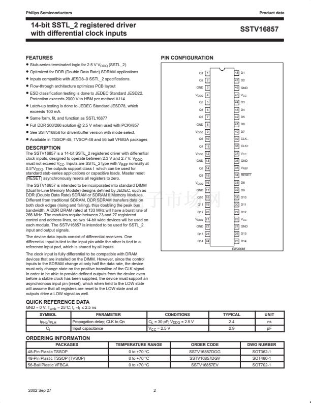
PIN CONFIGURATION
Q1
Q2
GND
V
DDQ
Q3
Q4
Q5
GND
V
DDQ
1
2
3
4
5
6
7
8
9
48 D1
47 D2
46 GND
45 V
CC
44 D3
43 D4
42 D5
41 D6
40 D7
39 CLK鈥?/div>
38 CLK+
37 V
CC
36 GND
35 V
REF
34 RESET
33 D8
32 D9
31 D10
30 D11
29 D12
28 V
CC
27 GND
26 D13
25 D14
Q6 10
Q7 11
V
DDQ
12
GND 13
Q8 14
Q9 15
V
DDQ
16
GND 17
Q10 18
Q11 19
Q12 20
V
DDQ
21
GND 22
Q13 23
Q14 24
SW00685
QUICK REFERENCE DATA
GND = 0 V; T
amb
= 25掳C; t
r
=t
f
v2.5
ns
SYMBOL
t
PHL
/t
PLH
C
I
PARAMETER
Propagation delay; CLK to Qn
Input capacitance
CONDITIONS
C
L
= 30 pF; V
DDQ
= 2.5 V
V
CC
= 2.5 V
TYPICAL
2.4
2.9
UNIT
ns
pF
ORDERING INFORMATION
PACKAGES
48-Pin Plastic TSSOP
48-Pin Plastic TSSOP (TVSOP)
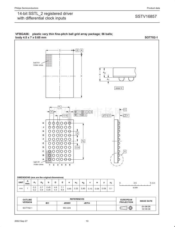
56-Ball Plastic VFBGA
TEMPERATURE RANGE
0 to +70
掳C
0 to +70
掳C
0 to +70
掳C
ORDER CODE
SSTV16857DGG
SSTV16857DGV
SSTV16857EV
DWG NUMBER
SOT362-1
SOT480-1
SOT702-1
2002 Sep 27
2


 1
1
 2
2
 3
3
 4
4
 5
5
 6
6
 7
7
 8
8
 9
9
 10
10
 11
11
 12
12
