鈥?/div>
ns
ns
MHz
ns
UNIT
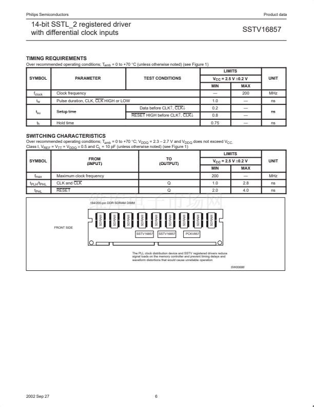
SWITCHING CHARACTERISTICS
Over recommended operating conditions; T
amb
= 0 to +70
掳C;
V
DDQ
= 2.3 鈥?2.7 V and V
DDQ
does not exceed V
CC.
Class I, V
REF
= V
TT
= V
DDQ
脳
0.5 and C
L
= 10 pF (unless otherwise noted) (see Figure 1)
LIMITS
SYMBOL
FROM
(INPUT)
Maximum clock frequency
CLK and CLK
RESET
184/200-pin DDR SDRAM DIMM
TO
(OUTPUT)
V
CC
= 2.5 V
卤0.2
V
MIN
MAX
鈥?/div>
2.8
4.0
200
UNIT
f
max
t
PLH
/t
PHL
t
PHL
MHz
ns
ns
Q
Q
1.0
2.0
SDRAM
SDRAM
SDRAM
SDRAM
SDRAM
SDRAM
SDRAM
SDRAM
FRONT SIDE
SSTV16857
SSTV16857
PCKV857
The PLL clock distribution device and SSTV registered drivers reduce
signal loads on the memory controller and prevent timing delays and
waveform distortions that would cause unreliable operation
SDRAM
SW00686
2002 Sep 27
6


 1
1
 2
2
 3
3
 4
4
 5
5
 6
6
 7
7
 8
8
 9
9
 10
10
 11
11
 12
12
