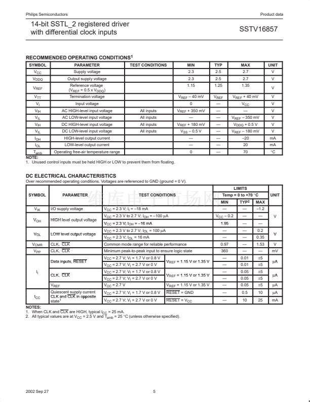
鈥?/div>
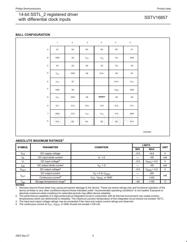
MAX
+4.6
鈥?0
V
DDQ
+ 0.5
鈥?0
V
DDQ
+ 0.5
卤50
卤100
UNIT
V
mA
V
mA
V
mA
T
stg
Storage temperature range
2
鈥?5
+150
掳C
NOTES:
1. Stresses beyond those listed may cause permanent damage to the device. These are stress ratings only and functional operation of the
device at these or any other conditions beyond those indicated under 鈥渞ecommended operating conditions鈥?is not implied. Exposure to
absolute-maximum-rated conditions for extended periods may affect device reliability.
2. The performance capability of a high-performance integrated circuit in conjunction with its thermal environment can create junction
temperatures which are detrimental to reliability. The maximum junction temperature of this integrated circuit should not exceed 150掳C.
3. The input and output voltage ratings may be exceeded if the input and output current ratings are observed.
4. The continuous current at V
CC
, V
DDQ
, or GND should not exceed
卤100
mA.
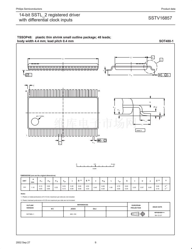
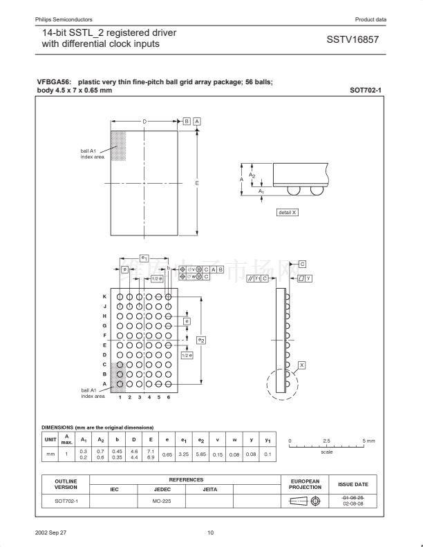
2002 Sep 27
4


 1
1
 2
2
 3
3
 4
4
 5
5
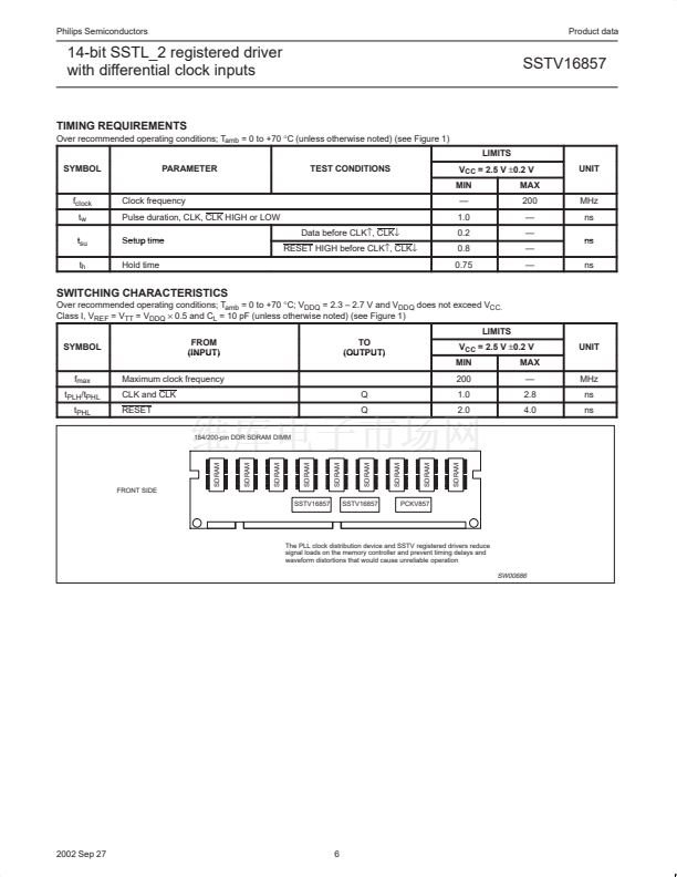 6
6
 7
7
 8
8
 9
9
 10
10
 11
11
 12
12
