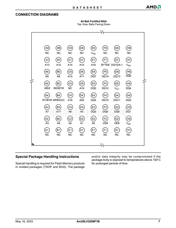
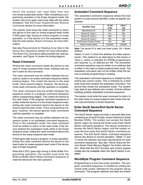
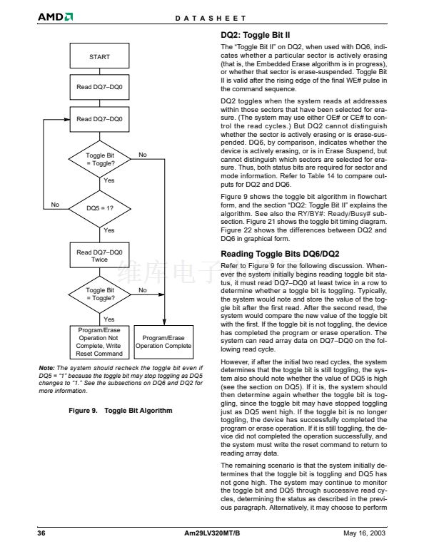
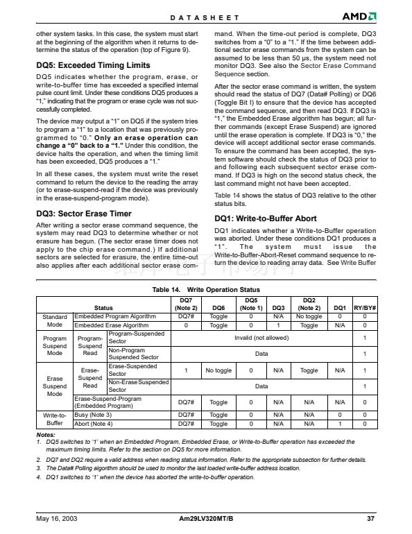
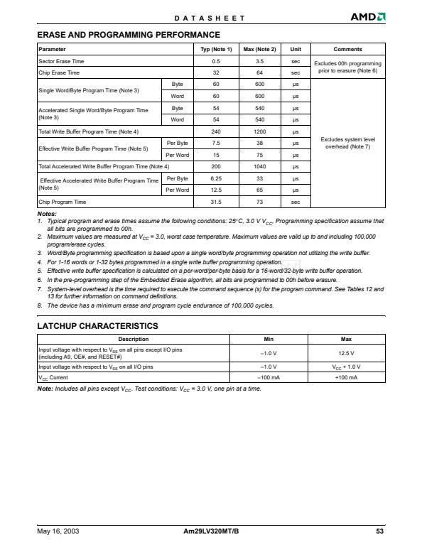
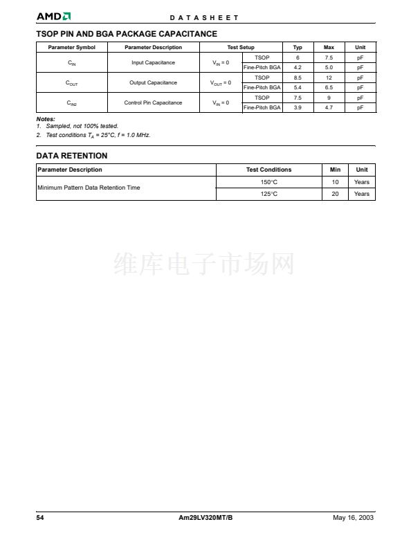
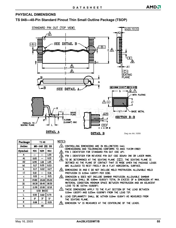
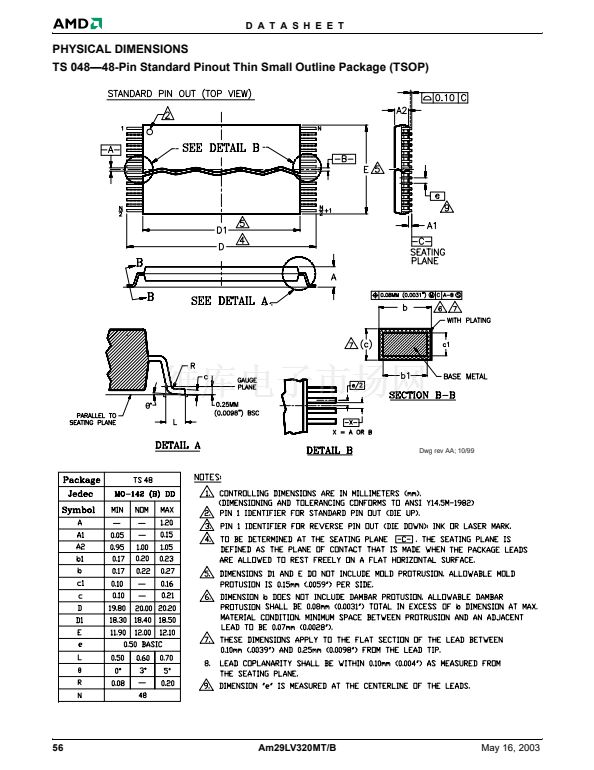
D A T A S H E E T
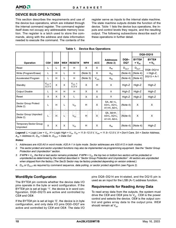
DEVICE BUS OPERATIONS
This section describes the requirements and use of
the device bus operations, which are initiated through
the internal command register. The command register
itself does not occupy any addressable memory loca-
tion. The register is a latch used to store the com-
mands, along with the address and data information
needed to execute the command. The contents of the
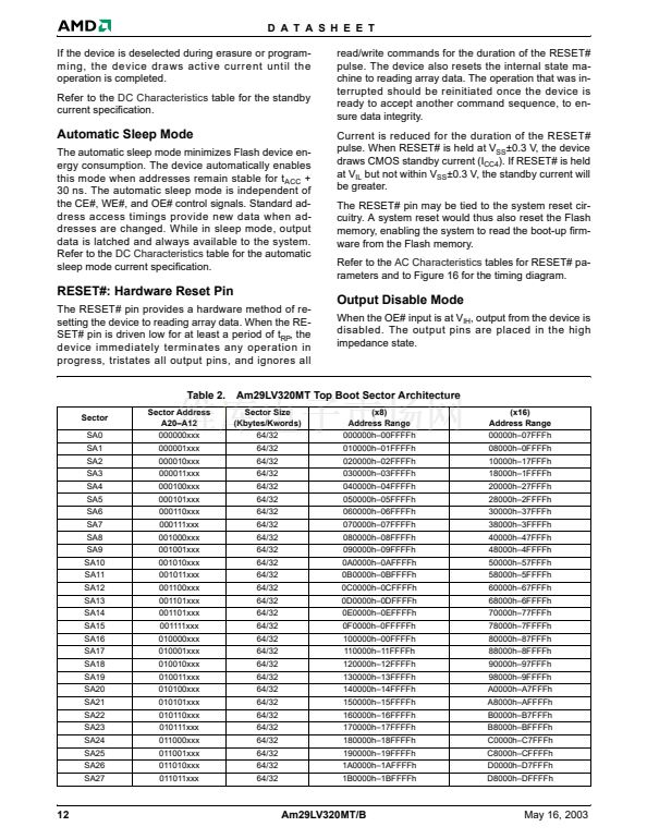
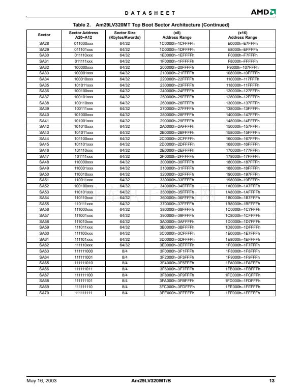
Table 1.
register serve as inputs to the internal state machine.
The state machine outputs dictate the function of the
device.
Table 1
lists the device bus operations, the in-
puts and control levels they require, and the resulting
output. The following subsections describe each of
these operations in further detail.
Device Bus Operations
DQ8鈥揇Q15
Operation
Read
Write (Program/Erase)
Accelerated Program
Standby
Output Disable
Reset
Sector Group Protect
(Note 2)
Sector Group Unprotect
(Note 2)
Temporary Sector Group
Unprotect
CE#
L
L
L
V
CC
卤
0.3 V
L
X
L
OE#
L
H
H
X
H
X
H
WE#
H
L
L
X
H
X
L
RESET#
H
H
H
V
CC
卤
0.3 V
H
L
V
ID
WP#
ACC
Addresses
(Note 2)
A
IN
A
IN
A
IN
X
X
X
SA, A6 =L,
A3=L, A2=L,
A1=H, A0=L
SA, A6=H,
A3=L, A2=L,
A1=H, A0=L
A
IN
DQ0鈥?/div>
DQ7
D
OUT
BYTE#
= V
IH
D
OUT
BYTE#
= V
IL
DQ8鈥揇Q14
= High-Z,
DQ15 = A-1
High-Z
High-Z
High-Z
X
X
(Note 3)
(Note 3)
X
X
X
H
X
X
V
HH
H
X
X
X
(Note 4) (Note 4)
(Note 4) (Note 4)
High-Z
High-Z
High-Z
(Note 4)
High-Z
High-Z
High-Z
X
L
H
L
V
ID
H
X
(Note 4)
X
X
X
X
X
V
ID
H
X
(Note 4) (Note 4)
High-Z
Legend:
L = Logic Low = V
IL
, H = Logic High = V
IH
, V
ID
= 11.5鈥?2.5 V, V
HH
= 11.5鈥?2.5 V, X = Don鈥檛 Care, SA = Sector Address,
A
IN
= Address In, D
IN
= Data In, D
OUT
= Data Out
Notes:
1. Addresses are A20:A0 in word mode; A20:A-1 in byte mode. Sector addresses are A20:A12 in both modes.
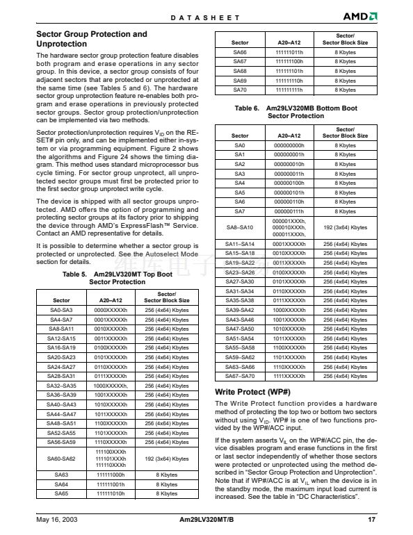
2. The sector protect and sector unprotect functions may also be implemented via programming equipment. See the 鈥淪ector Group
Protection and Unprotection鈥?section.
3. If WP# = V
IL
, the first or last sector remains protected. If WP# = V
IH
, the top two or bottom two sectors will be protected or
unprotected as determined by the method described in 鈥淪ector Group Protection and Unprotection鈥? All sectors are unprotected
when shipped from the factory (The SecSi Sector may be factory protected depending on version ordered.)
4. D
IN
or D
OUT
as required by command sequence, data polling, or sector protect algorithm (see Figure 2).
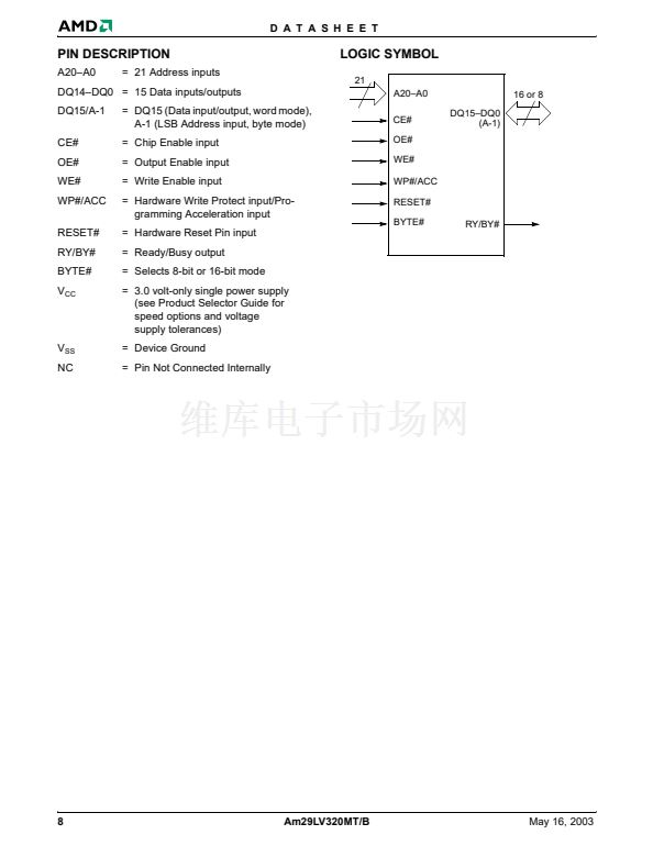
Word/Byte Configuration
The BYTE# pin controls whether the device data I/O
pins operate in the byte or word configuration. If the
BYTE# pin is set at logic 鈥?鈥? the device is in word con-
figuration, DQ0鈥揇Q15 are active and controlled by
CE# and OE#.
If the BYTE# pin is set at logic 鈥?鈥? the device is in byte
configuration, and only data I/O pins DQ0鈥揇Q7 are
active and controlled by CE# and OE#. The data I/O
pins DQ8鈥揇Q14 are tri-stated, and the DQ15 pin is
used as an input for the LSB (A-1) address function.
Requirements for Reading Array Data
To read array data from the outputs, the system must
drive the CE# and OE# pins to V
IL
. CE# is the power
control and selects the device. OE# is the output con-
trol and gates array data to the output pins. WE#
should remain at V
IH
.
10
Am29LV320MT/B
May 16, 2003


 1
1
 2
2
 3
3
 4
4
 5
5
 6
6
 7
7
 8
8
 9
9
 10
10
 11
11
 12
12
 13
13
 14
14
 15
15
 16
16
 17
17
 18
18
 19
19
 20
20
 21
21
 22
22
 23
23
 24
24
 25
25
 26
26
 27
27
 28
28
 29
29
 30
30
 31
31
 32
32
 33
33
 34
34
 35
35
 36
36
 37
37
 38
38
 39
39
 40
40
 41
41
 42
42
 43
43
 44
44
 45
45
 46
46
 47
47
 48
48
 49
49
 50
50
 51
51
 52
52
 53
53
 54
54
 55
55
 56
56
 57
57
 58
58
 59
59
 60
60
 61
61
