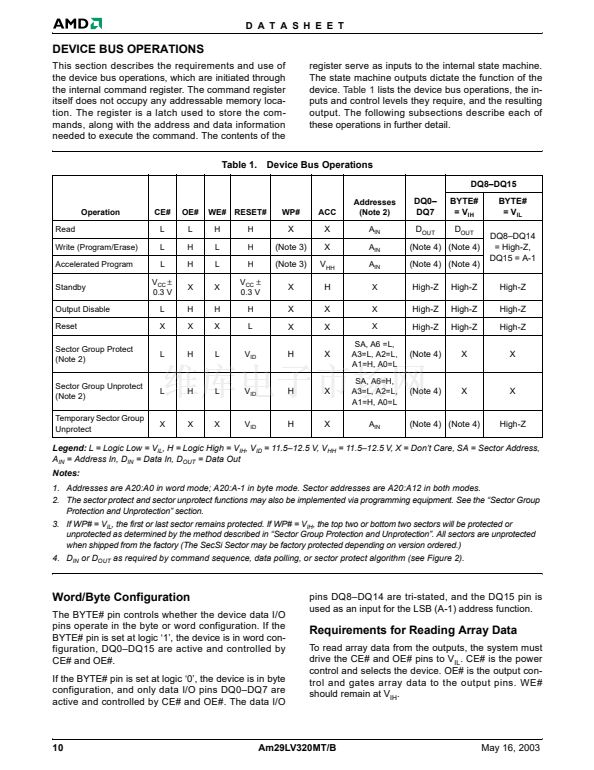
D A T A S H E E T
If the device is deselected during erasure or program-
ming, the device draws active current until the
operation is completed.
Refer to the
DC Characteristics
table for the standby
current specification.
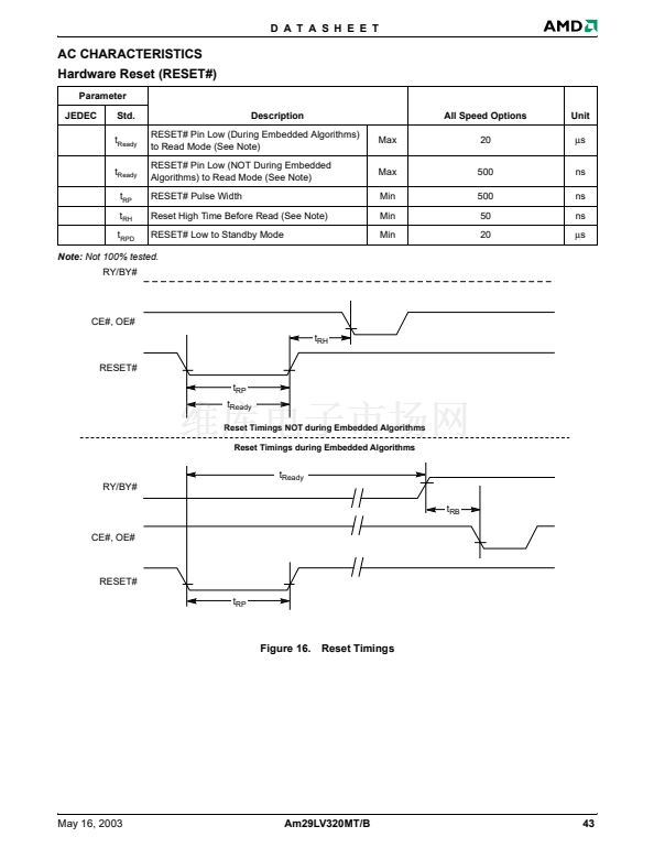
read/write commands for the duration of the RESET#
pulse. The device also resets the internal state ma-
chine to reading array data. The operation that was in-
terrupted should be reinitiated once the device is
ready to accept another command sequence, to en-
sure data integrity.
Current is reduced for the duration of the RESET#
pulse. When RESET# is held at V
SS
卤0.3 V, the device
draws CMOS standby current (I
CC4
). If RESET# is held
at V
IL
but not within V
SS
卤0.3 V, the standby current will
be greater.
The RESET# pin may be tied to the system reset cir-
cuitry. A system reset would thus also reset the Flash
memory, enabling the system to read the boot-up firm-
ware from the Flash memory.
Refer to the
AC Characteristics
tables for RESET# pa-
rameters and to Figure 16 for the timing diagram.
Automatic Sleep Mode
The automatic sleep mode minimizes Flash device en-
ergy consumption. The device automatically enables
this mode when addresses remain stable for t
ACC
+
30 ns. The automatic sleep mode is independent of
the CE#, WE#, and OE# control signals. Standard ad-
dress access timings provide new data when ad-
dresses are changed. While in sleep mode, output
data is latched and always available to the system.
Refer to the
DC Characteristics
table for the automatic
sleep mode current specification.
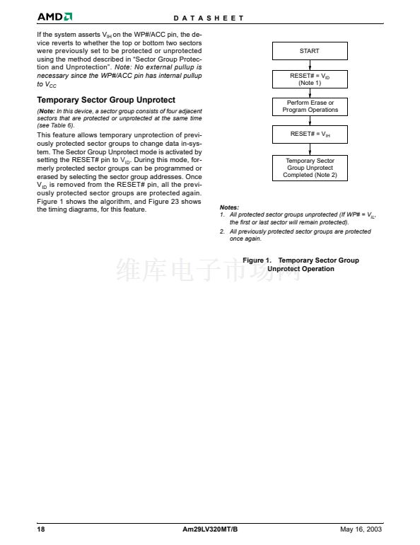
RESET#: Hardware Reset Pin
The RESET# pin provides a hardware method of re-
setting the device to reading array data. When the RE-
SET# pin is driven low for at least a period of t
RP
, the
device immediately terminates any operation in
progress, tristates all output pins, and ignores all
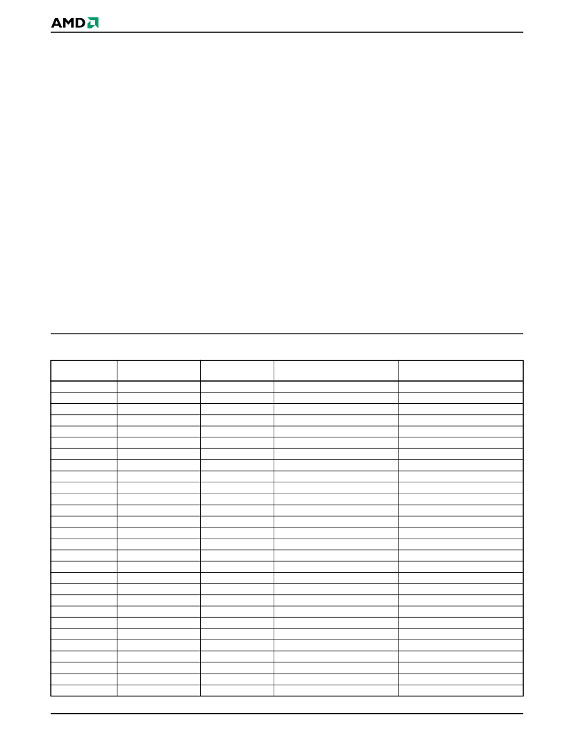
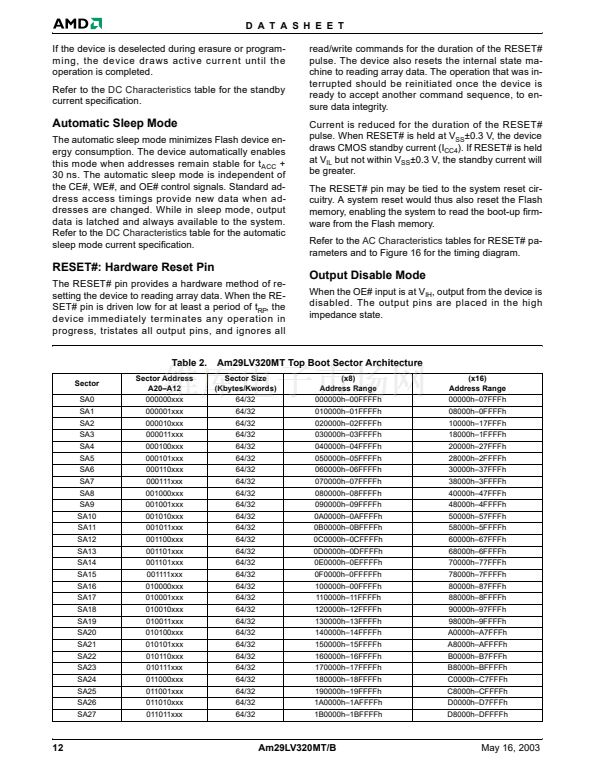
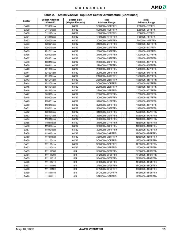
Table 2.
Sector
SA0
SA1
SA2
SA3
SA4
SA5
SA6
SA7
SA8
SA9
SA10
SA11
SA12
SA13
SA14
SA15
SA16
SA17
SA18
SA19
SA20
SA21
SA22
SA23
SA24
SA25
SA26
SA27
Sector Address
A20鈥揂12
000000xxx
000001xxx
000010xxx
000011xxx
000100xxx
000101xxx
000110xxx
000111xxx
001000xxx
001001xxx
001010xxx
001011xxx
001100xxx
001101xxx
001101xxx
001111xxx
010000xxx
010001xxx
010010xxx
010011xxx
010100xxx
010101xxx
010110xxx
010111xxx
011000xxx
011001xxx
011010xxx
011011xxx
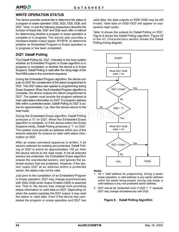
Output Disable Mode
When the OE# input is at V
IH
, output from the device is
disabled. The output pins are placed in the high
impedance state.
Am29LV320MT Top Boot Sector Architecture
Sector Size
(Kbytes/Kwords)
64/32
64/32
64/32
64/32
64/32
64/32
64/32
64/32
64/32
64/32
64/32
64/32
64/32
64/32
64/32
64/32
64/32
64/32
64/32
64/32
64/32
64/32
64/32
64/32
64/32
64/32
64/32
64/32
(x8)
Address Range
000000h鈥?0FFFFh
010000h鈥?1FFFFh
020000h鈥?2FFFFh
030000h鈥?3FFFFh
040000h鈥?4FFFFh
050000h鈥?5FFFFh
060000h鈥?6FFFFh
070000h鈥?7FFFFh
080000h鈥?8FFFFh
090000h鈥?9FFFFh
0A0000h鈥?AFFFFh
0B0000h鈥?BFFFFh
0C0000h鈥?CFFFFh
0D0000h鈥?DFFFFh
0E0000h鈥?EFFFFh
0F0000h鈥?FFFFFh
100000h鈥?0FFFFh
110000h鈥?1FFFFh
120000h鈥?2FFFFh
130000h鈥?3FFFFh
140000h鈥?4FFFFh
150000h鈥?5FFFFh
160000h鈥?6FFFFh
170000h鈥?7FFFFh
180000h鈥?8FFFFh
190000h鈥?9FFFFh
1A0000h鈥?AFFFFh
1B0000h鈥?BFFFFh
(x16)
Address Range
00000h鈥?7FFFh
08000h鈥?FFFFh
10000h鈥?7FFFh
18000h鈥?FFFFh
20000h鈥?7FFFh
28000h鈥?FFFFh
30000h鈥?7FFFh
38000h鈥?FFFFh
40000h鈥?7FFFh
48000h鈥?FFFFh
50000h鈥?7FFFh
58000h鈥?FFFFh
60000h鈥?7FFFh
68000h鈥?FFFFh
70000h鈥?7FFFh
78000h鈥?FFFFh
80000h鈥?7FFFh
88000h鈥?FFFFh
90000h鈥?7FFFh
98000h鈥?FFFFh
A0000h鈥揂7FFFh
A8000h鈥揂FFFFh
B0000h鈥揃7FFFh
B8000h鈥揃FFFFh
C0000h鈥揅7FFFh
C8000h鈥揅FFFFh
D0000h鈥揇7FFFh
D8000h鈥揇FFFFh
12
Am29LV320MT/B
May 16, 2003


 1
1
 2
2
 3
3
 4
4
 5
5
 6
6
 7
7
 8
8
 9
9
 10
10
 11
11
 12
12
 13
13
 14
14
 15
15
 16
16
 17
17
 18
18
 19
19
 20
20
 21
21
 22
22
 23
23
 24
24
 25
25
 26
26
 27
27
 28
28
 29
29
 30
30
 31
31
 32
32
 33
33
 34
34
 35
35
 36
36
 37
37
 38
38
 39
39
 40
40
 41
41
 42
42
 43
43
 44
44
 45
45
 46
46
 47
47
 48
48
 49
49
 50
50
 51
51
 52
52
 53
53
 54
54
 55
55
 56
56
 57
57
 58
58
 59
59
 60
60
 61
61
