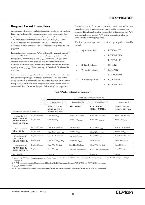
the table. The second request is shown along the horizontal
axis at the top of the table. Each request includes a bank speci-
same, or they may be different. These two subcases for each
interaction are shown along the vertical axis on the left.
There are 32 possible interaction cases altogether. The table
gives each case a label of the form 鈥渪yz鈥? where 鈥渪鈥?and 鈥測鈥?/div>
are one of the four operation types (鈥淎鈥?for Activate, 鈥淩鈥?for
Read, 鈥淲鈥?for Write, or 鈥淧鈥?for Precharge) for the first and
second request, respectively, and 鈥渮鈥?indicates the same bank
(鈥渟鈥? or different bank (鈥渄鈥?.
Along the horizontal axis at the bottom of the table are cross
references to four figures (Figure 4 through Figure 7). Each
figure illustrates the eight cases in the corresponding vertical
column. Thus, Figure 4 shows the eight cases when the second
request is an activate operation (鈥淎鈥?. In the following discus-
sion of the cases, only those in which the interaction interval is
greater than t
CYCLE
will be described.
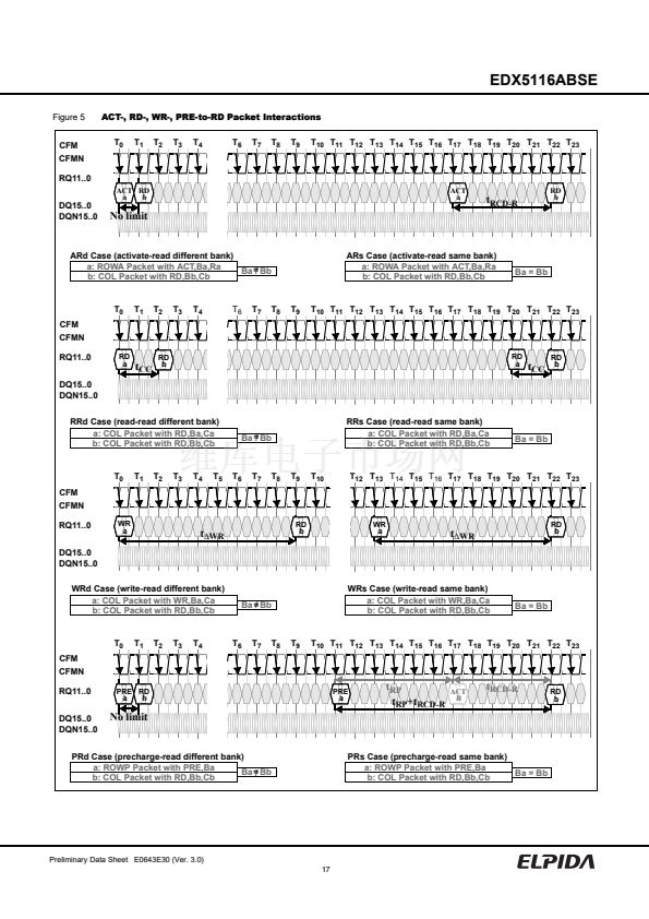
minimum interval between two read operations.
The interaction interval for the WRd and WRs cases is t
鈭哤R
.
This is the write-to-read time parameter and represents the
minimum interval between a write and a read operation to any
banks. See 鈥淩ead/Write Interaction鈥?on page 28.
The interaction interval for the PRs case is t
RP
+ t
RCD-R
. An
activate operation must be inserted between the precharge and
the read operation. The minimum interval between a precharge
and an activate operation to a bank is t
RP
. The minimum inter-
val between an activate and read operation to a bank is t
RCD-R
.
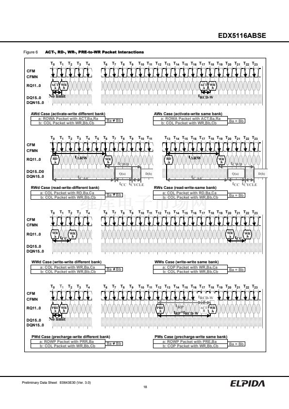
In Figure 6, the interaction interval for the AWs case is t
RCD-W
.
This is the row-to-column-write timing parameter and repre-
sents the minimum interval between an activate operation and
a write operation to a bank.
The interaction interval for the RWd and RWs cases is t
鈭哛W
.
This is the read-to-write time parameter and represents the
minimum interval between a read and a write operation to any
banks. See 鈥淩ead/Write Interaction鈥?on page 28.
The interaction interval for the WWd and WWs cases is t
CC
.
This is the column-to-column time parameter and represents
the minimum interval between two write operations.
The interaction interval for the PWs case is t
RP
+ t
RCD-W
. An
activate operation must be inserted between the precharge and
the write operation. The minimum interval between a pre-
charge and an activate operation to a bank is t
RP
. The mini-
mum interval between an activate and a write operation to a
bank is t
RCD-W
.
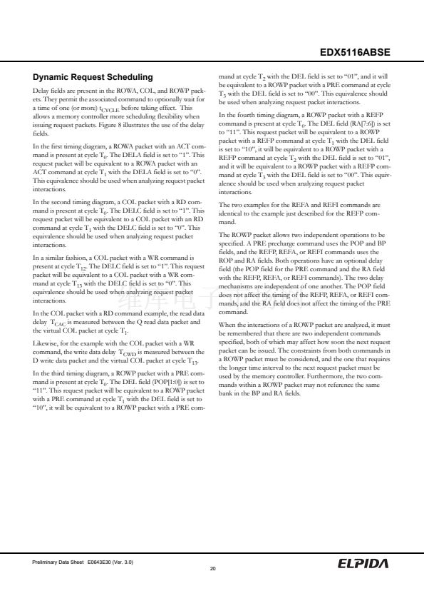
In Figure 7, the interaction interval for the APs case is t
RAS
.
This parameter is the minimum activate-to-precharge time to a
bank.
The interaction intervals for the RPs and WPs cases are t
RDP
and t
WDP
, respectively. These are the read- or write-to-pre-
charge time parameters to a bank.
The interaction interval for the PPd case is t
PP
. This parameter
is the precharge-to-precharge time and the minimum interval
between precharge commands to different banks of a device.
The interaction interval for the PPs case is t
RC
. This is the row
cycle time parameter and the minimum interval between pre-
charge commands to same banks of a device. An activate oper-
ation must be inserted between the two activate operations.
This activate operation must be placed a time t
RP
after the first,
and a time t
RAS
before the second precharge.
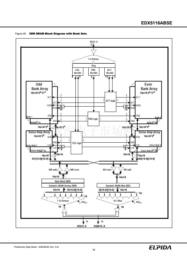
Request Interaction Cases
In Figure 4, the interaction interval for the AAd case is t
RR
.
This parameter is the row-to-row time and is the minimum
interval between activate commands to different banks of a
device.
The interaction interval for the AAs case is t
RC
. This is the
row cycle time parameter and is the minimum interval between
activate commands to same banks of a device. A precharge
operation must be inserted between the two activate opera-
tions.
The interaction interval for the RAs case is t
RDP
+ t
RP
. A pre-
charge operation must be inserted between the read and acti-
vate operation. The minimum interval between a read and a
precharge operation to a bank is t
RDP
. The minimum interval
between a precharge and an activate operation to a bank is t
RP
.
The interaction interval for the WAs case is t
WDP
+ t
RP
. A
precharge operation must be inserted between the read and the
activate operation.The minimum interval between a write and a
precharge operation to a bank is t
WDP
. The minimum interval
between a precharge and an activate operation to a bank is t
RP
.
The interaction interval for the PAs case is t
RP
. The minimum
interval between a precharge and an activate operation to a
bank is t
RP
.
In Figure 5, the interaction interval for the ARs case is t
RCD-R
.
This is the row-to-column-read time parameter and represents
the minimum interval between an activate operation and a read
operation to a bank.
The interaction interval for the RRd and RRs cases is t
CC
. This
is the column-to-column time parameter and represents the
Preliminary Data Sheet E0643E30 (Ver. 3.0)
15


 1
1
 2
2
 3
3
 4
4
 5
5
 6
6
 7
7
 8
8
 9
9
 10
10
 11
11
 12
12
 13
13
 14
14
 15
15
 16
16
 17
17
 18
18
 19
19
 20
20
 21
21
 22
22
 23
23
 24
24
 25
25
 26
26
 27
27
 28
28
 29
29
 30
30
 31
31
 32
32
 33
33
 34
34
 35
35
 36
36
 37
37
 38
38
 39
39
 40
40
 41
41
 42
42
 43
43
 44
44
 45
45
 46
46
 47
47
 48
48
 49
49
 50
50
 51
51
 52
52
 53
53
 54
54
 55
55
 56
56
 57
57
 58
58
 59
59
 60
60
 61
61
 62
62
 63
63
 64
64
 65
65
 66
66
 67
67
 68
68
 69
69
 70
70
 71
71
 72
72
 73
73
 74
74
 75
75
 76
76
 77
77
 78
78
