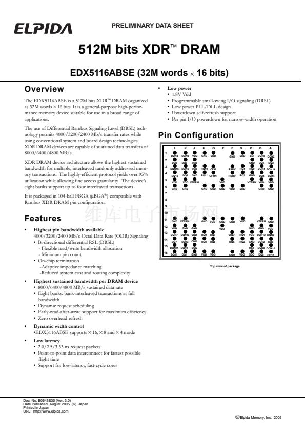
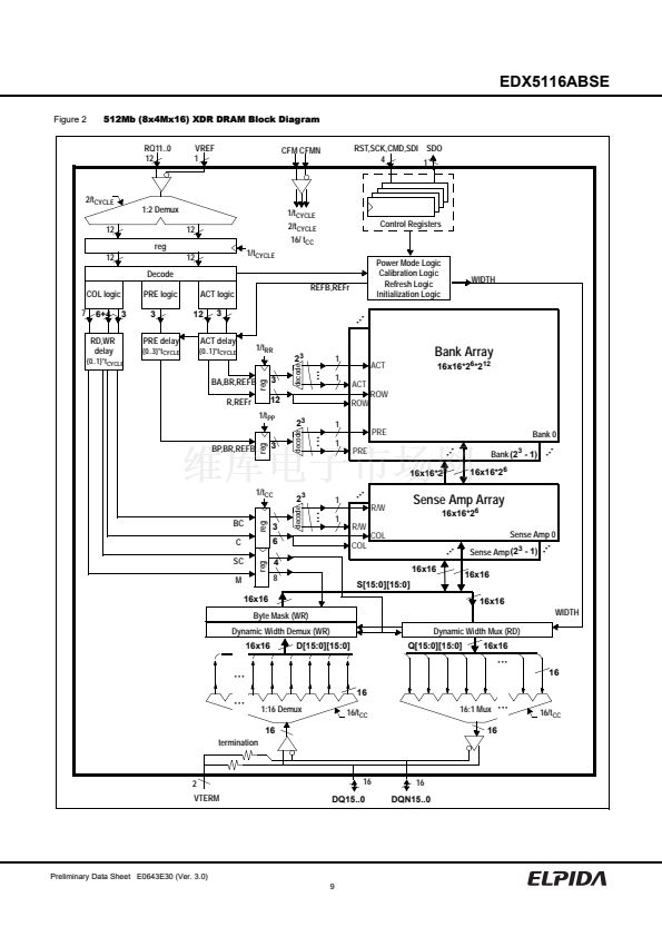
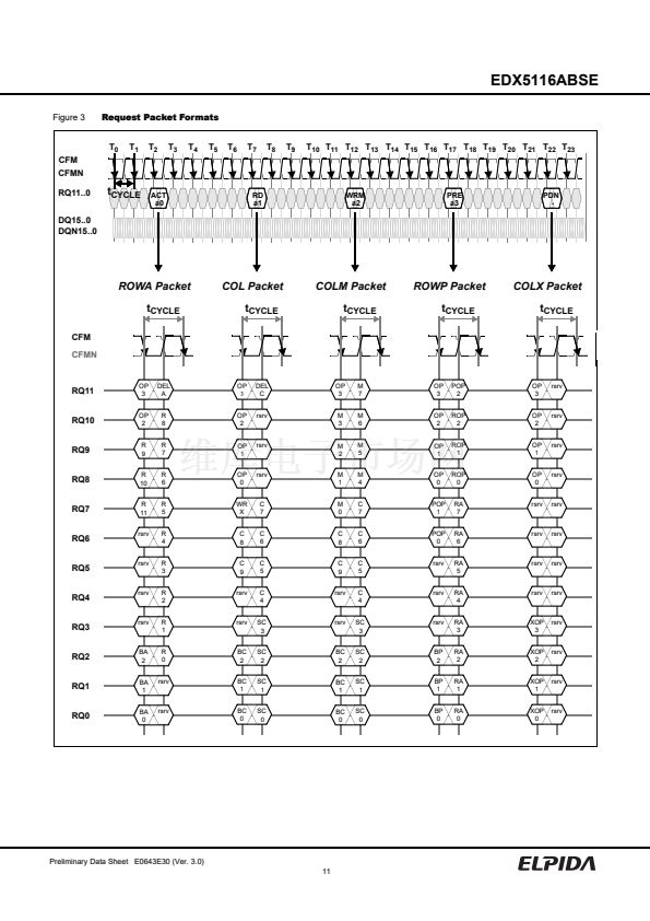
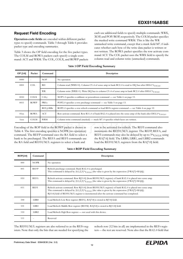
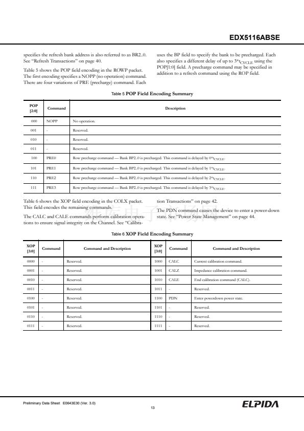
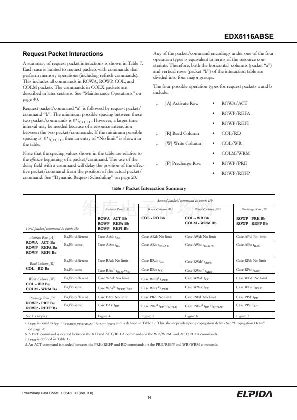
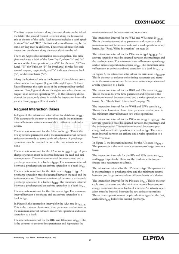
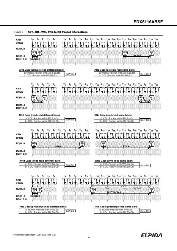
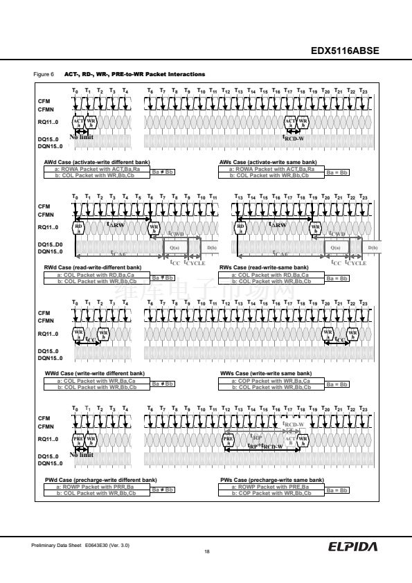
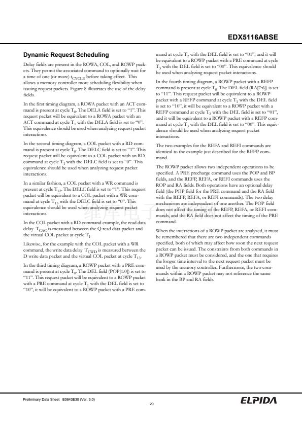
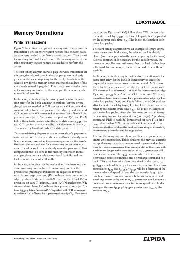
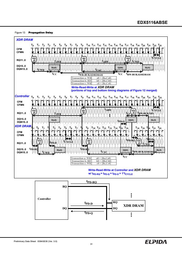
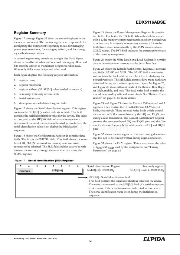
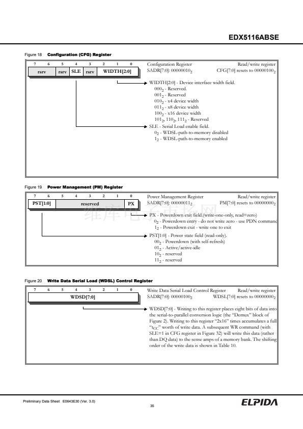
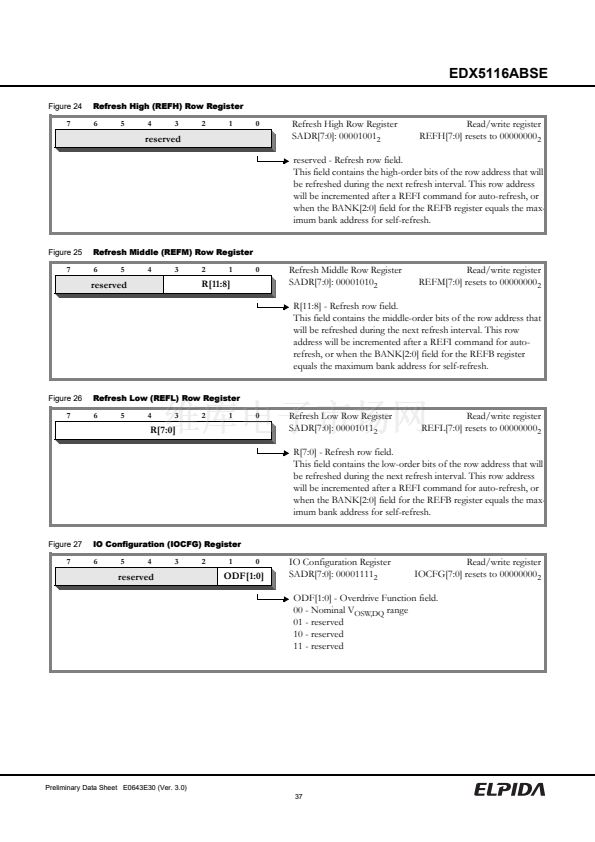
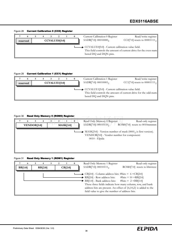
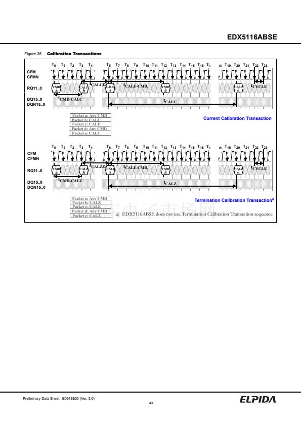
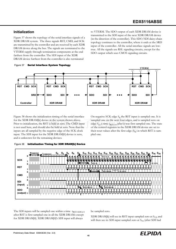
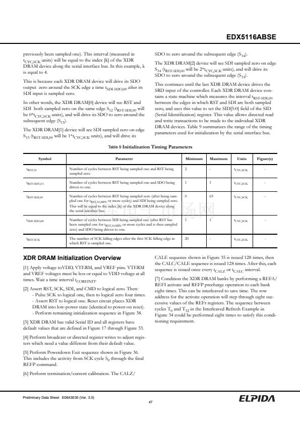
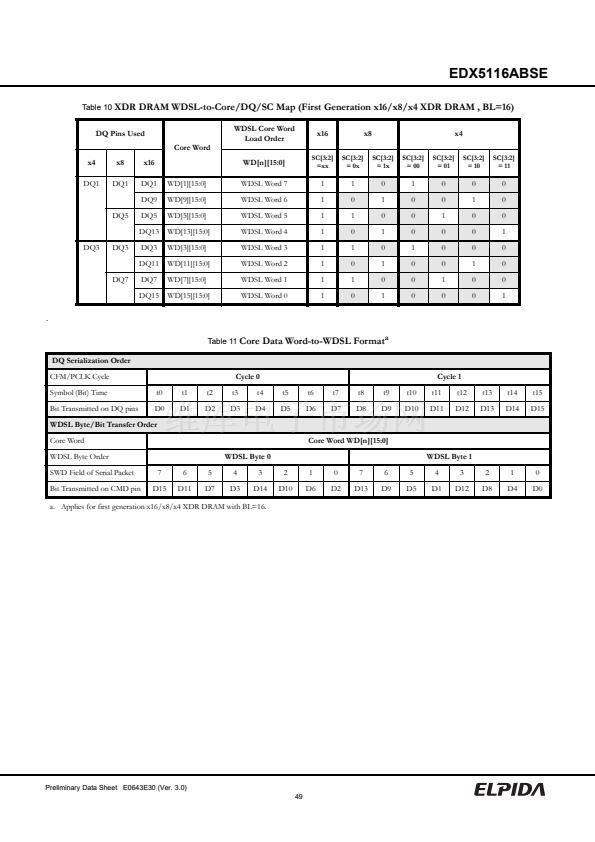
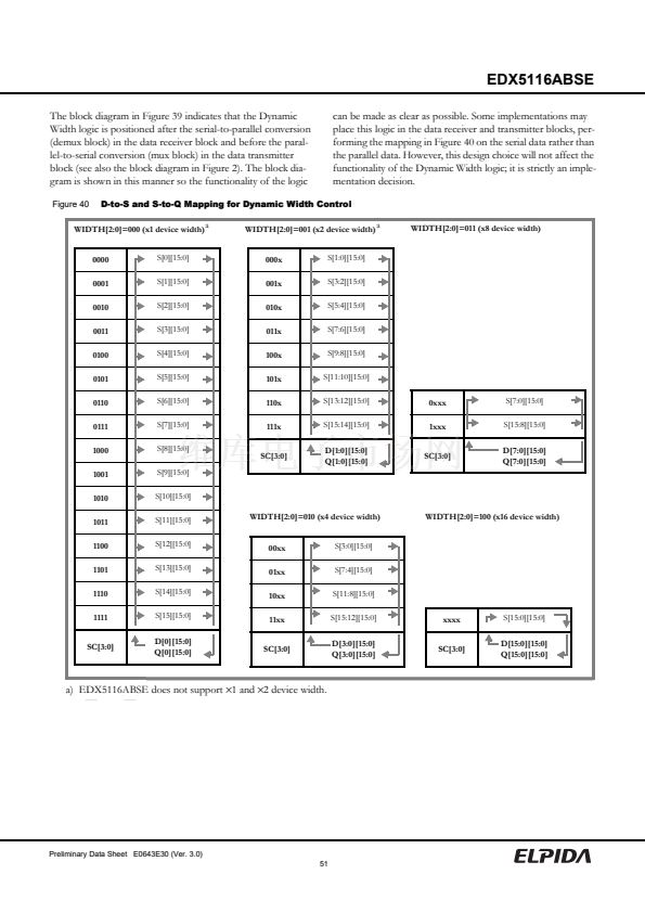
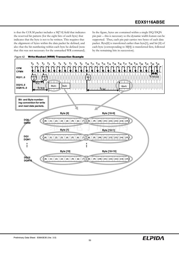
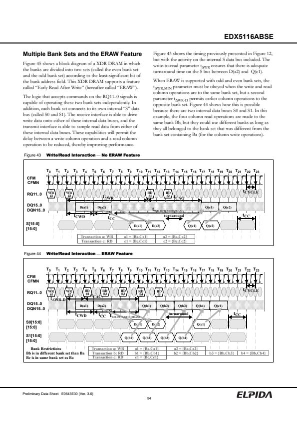
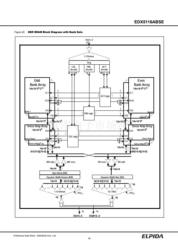
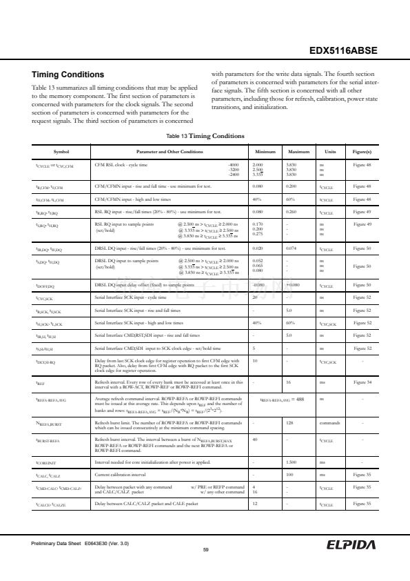
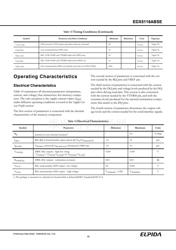
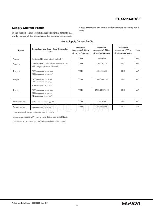
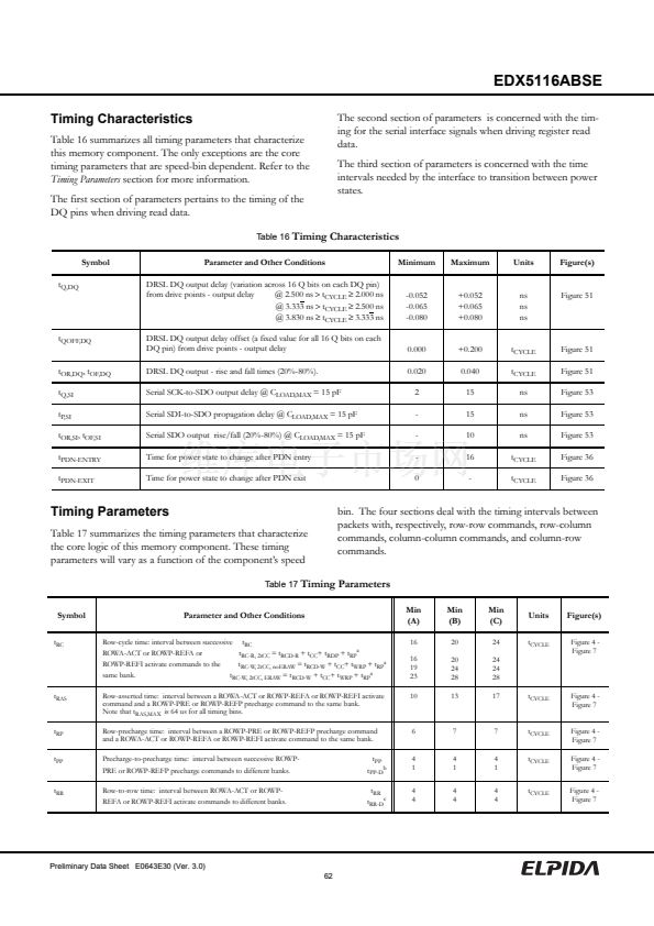
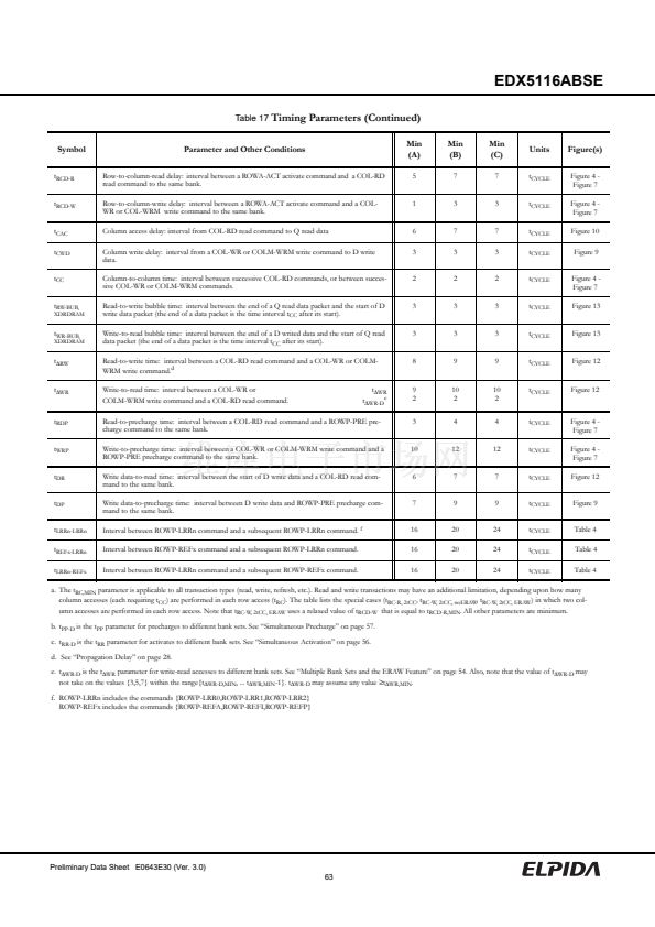
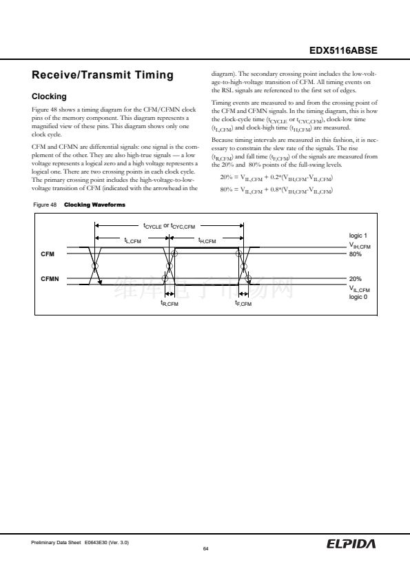
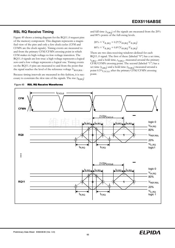
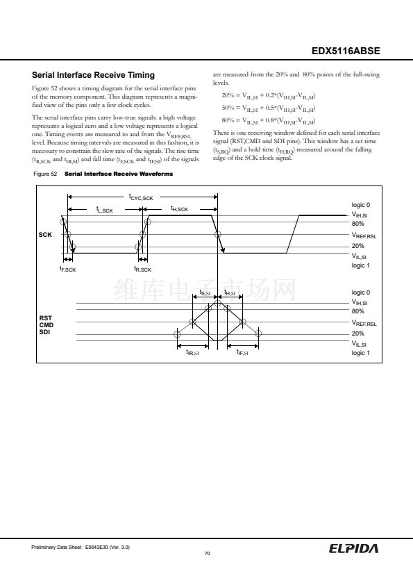
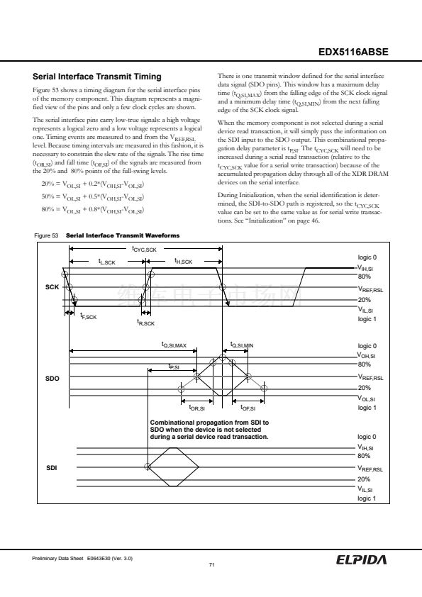
EDX5116ABSE
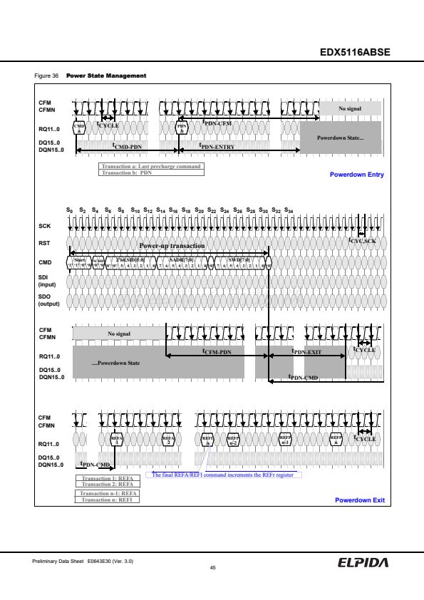
Power State Management
Figure 36 shows power state transition diagrams for the XDR
DRAM device. There are two power states in the XDR
DRAM: Powerdown and Active. Powerdown state is to be used
in applications in which it is necessary to shut down the CFM/
CFMN clock signals. In this state, the contents of the storage
cells of the XDR DRAM will be retained by an internal state
machine which performs periodic refresh operations using the
REFB and REFr control registers.
The upper diagram shows the sequence needed for Power-
down entry. Prior to starting the sequence, all banks of the
XDR DRAM must be precharged so they are left in a closed
state. Also, all 2
3
banks must be refreshed using the current
value of the REFr registers,
and the REFr registers must NOT be
incremented with the REFI command at the end of this special set of
refresh transactions.
This ensures that no matter what value has
been left in the REFB register, no row of any bank will be
skipped when automatic refresh is first started in Powerdown.
There may be some banks at the current row value in the REFr
registers that are refreshed twice during the Powerdown entry
process.
After the last request packet (with the command CMDa in the
upper diagram of the figure), an interval of t
CMD-PDN
is
observed. No request packets should be issued during this
period.
A COLX packet with the PDN command is issued after this
interval, causing the XDR DRAM to enter Powerdown state
after an interval of t
PDN-ENTRY
has elapsed (this is the parame-
ter that should be used for calculating the power dissipation of
the XDR DRAM). The CFM/CFMN clock signals may be
removed a time t
PDN-CFM
after the COLX packet with the
PDN command. Also, the termination voltage supply may be
removed (set to the ground reference) from the VTERM pins a
time t
PDN-CFM
after the COLX packet with the PDN com-
mand. The voltage on the DQ/DQN pins will follow the volt-
age on the VTERM pins during Powerdown entry.
When the XDR DRAM is in Powerdown, an internal fre-
quency source and state machine will automatically generate
internal refresh transactions. It will cycle through all 2
3
state
combinations of the REFB register. When the largest value is
reached and the REFB value wraps around, the REFr register
is incremented to the next value. The REFB and REFr values
select which bank and which row are refreshed during the next
automatic refresh transaction.
The lower diagram shows the sequence needed for Powerdown
exit. The sequence is started with a serial broadcast write (SBW
command) transaction using the serial bus of the XDR
DRAM. This transaction writes the value 鈥?0000001鈥?to the
Power Management (PM) register (SADR=鈥?0000011鈥? of all
XDR DRAMs connected to the serial bus. This sets the PX bit
of the PM register, causing the XDR DRAMs to return to
Active power state.
The CFM/CFMN clock signals must be stable a time t
CFM-
PDN
before the end of the SBW transaction. Also, the termina-
tion voltage supply must be restored to its normal operating
point (V
TERM,DRSL
) on the VTERM pins a time t
CFM-PDN
before the end of the SBW transaction. The voltage on the
DQ/DQN pins will follow the voltage on the VTERM pins
during Powerdown exit.
The XDR DRAM will enter Active state after an interval of
t
PDN-EXIT
has elapsed from the end of the SBW transaction
(this is the parameter that should be used for calculating the
power dissipation of the XDR DRAM).
The first request packet may be issued after an interval of
t
PDN-CMD
has elapsed from the end of the SBW transaction,
and must contain a 鈥淩EFA鈥?command in a ROWP packet.
In this
example, this packet is denoted with the command 鈥淩EFA 1鈥?
No other request packets should be issued during this t
PDN-
CMD
interval.
All 鈥渘鈥?banks (in the example, n=2
3
) must be refreshed using
the current value of the REFr registers. The 鈥渘th鈥?refresh
transaction will use a 鈥淩EFI鈥?command to increment the
REFr register (instead of a 鈥淩EFR鈥?command). This ensures
that no matter what value has been left in the REFB register,
no row of any bank will be skipped when normal refresh is
restarted in Active state. There may be some banks at the cur-
rent row value in the REFr registers that are refreshed twice
during the Powerdown exit process.
Note that during the Powerdown state an internal time source
keeps the device refreshed. However, during the t
PDN-CMD
interval, no internal refresh operations are performed. As a
result, an additional burst of refresh transactions must be
issued after the burst of 鈥渘鈥?transactions described above.
This second burst consists of 鈥渕鈥?refresh transactions:
m = ceiling[2
3
*2
12
*t
PDN-CMD
/t
REF
]
Where 鈥?
12
鈥?is the number of rows per bank, and 鈥?
3
鈥?is the
number of banks. Every 鈥渘th鈥?refresh transaction (where
n=2
3
) will use a 鈥淩EFI鈥?command (to increment the REFr
register) instead of a 鈥淩EFA鈥?command.
Preliminary Data Sheet E0643E30 (Ver. 3.0)
44


 1
1
 2
2
 3
3
 4
4
 5
5
 6
6
 7
7
 8
8
 9
9
 10
10
 11
11
 12
12
 13
13
 14
14
 15
15
 16
16
 17
17
 18
18
 19
19
 20
20
 21
21
 22
22
 23
23
 24
24
 25
25
 26
26
 27
27
 28
28
 29
29
 30
30
 31
31
 32
32
 33
33
 34
34
 35
35
 36
36
 37
37
 38
38
 39
39
 40
40
 41
41
 42
42
 43
43
 44
44
 45
45
 46
46
 47
47
 48
48
 49
49
 50
50
 51
51
 52
52
 53
53
 54
54
 55
55
 56
56
 57
57
 58
58
 59
59
 60
60
 61
61
 62
62
 63
63
 64
64
 65
65
 66
66
 67
67
 68
68
 69
69
 70
70
 71
71
 72
72
 73
73
 74
74
 75
75
 76
76
 77
77
 78
78
