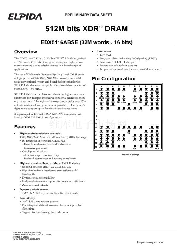
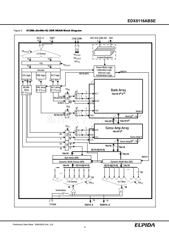
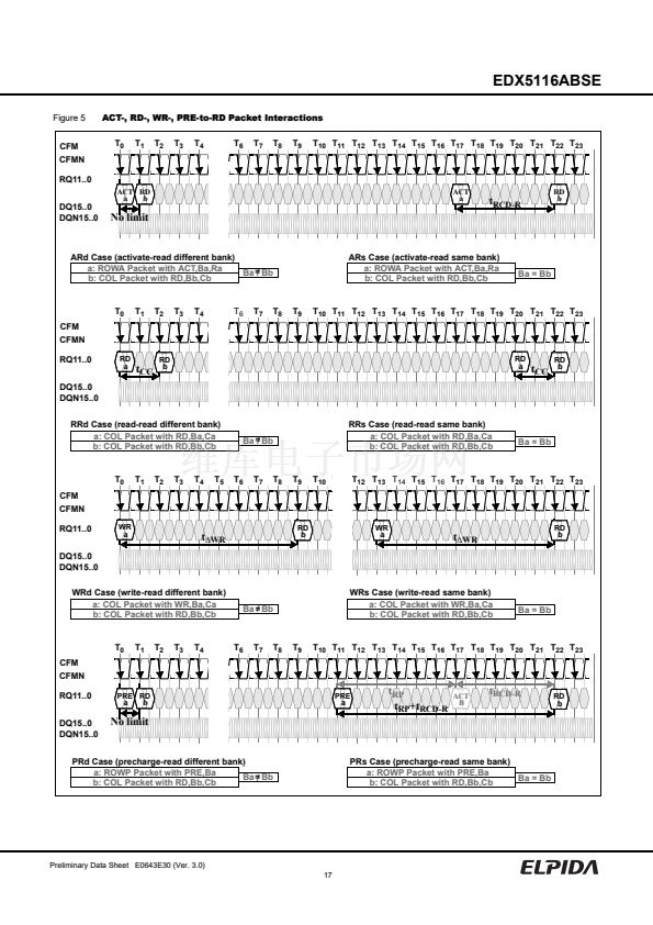
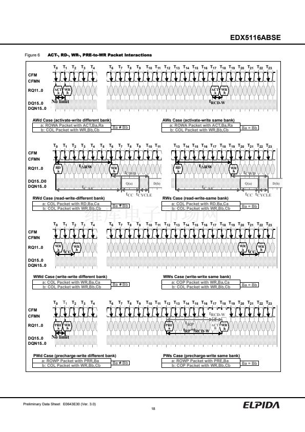
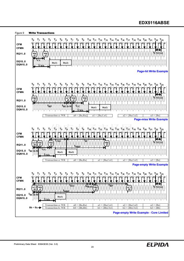
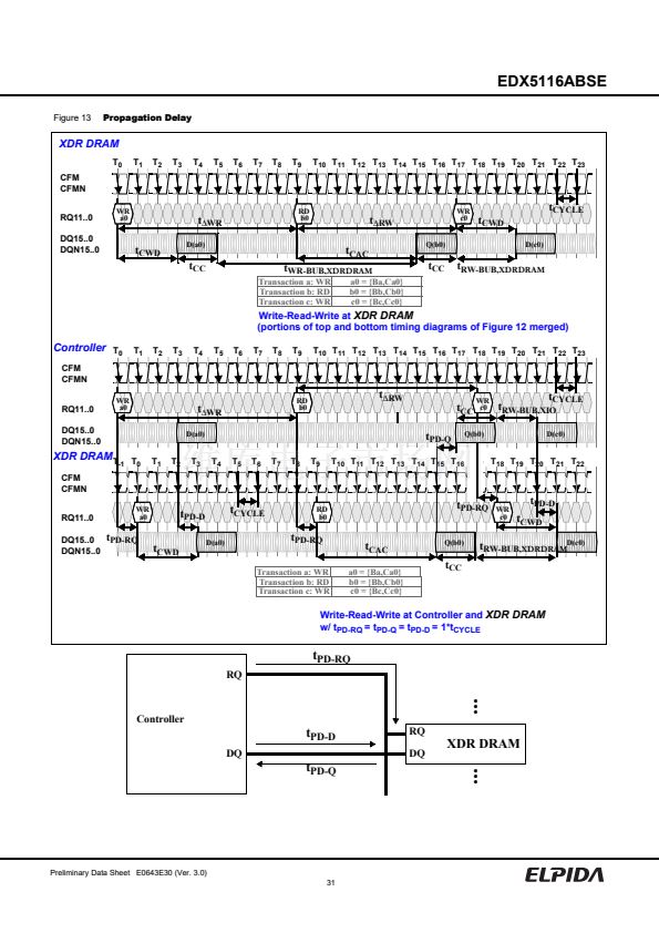
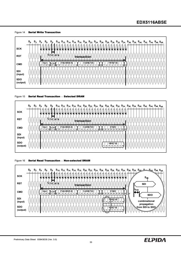
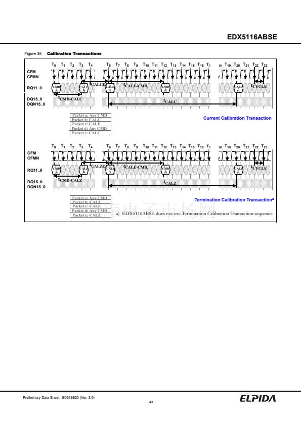
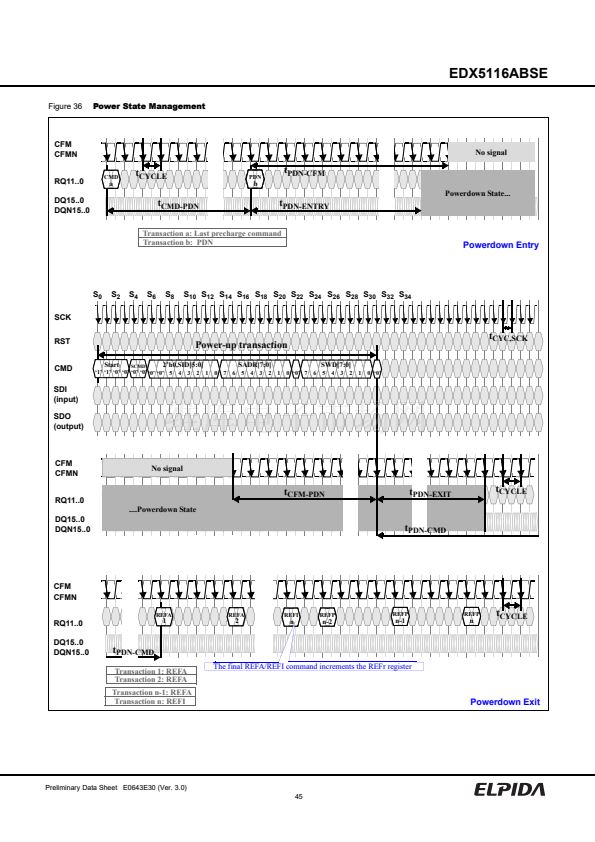
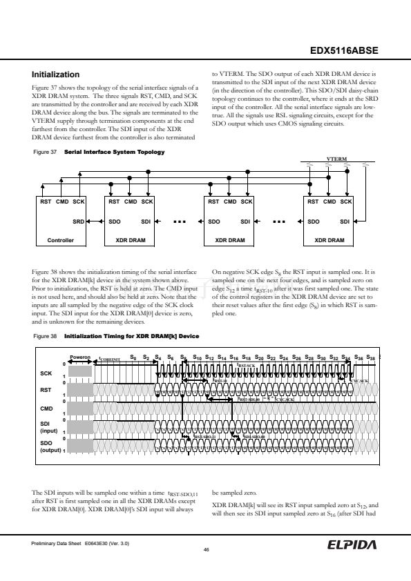
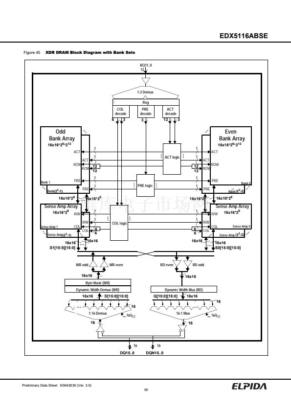
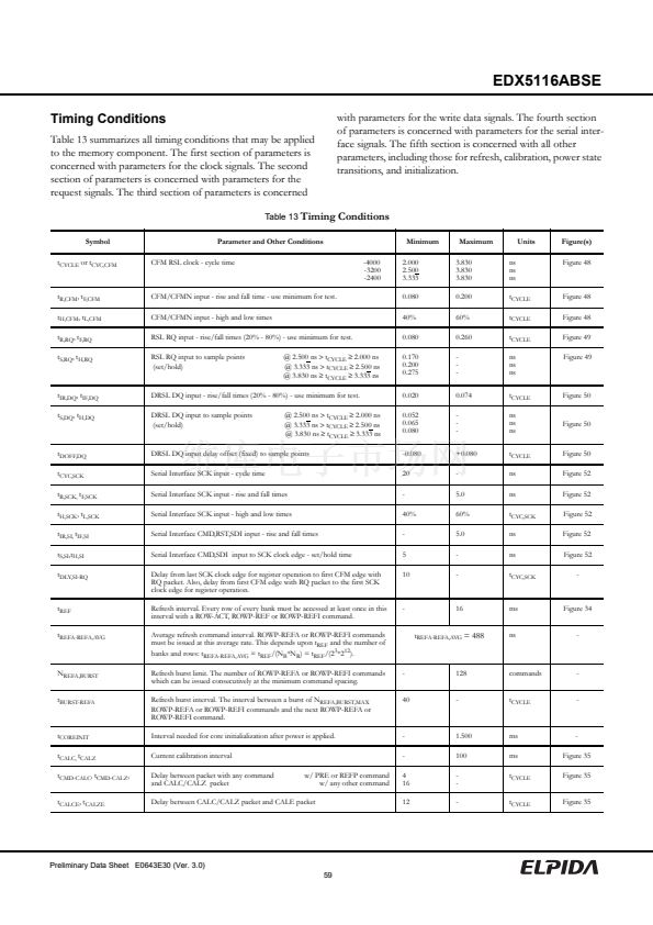
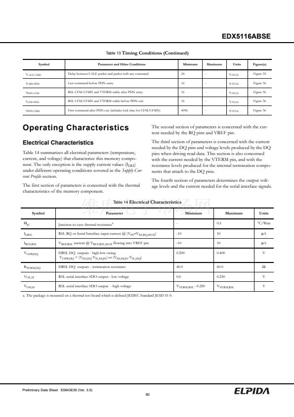
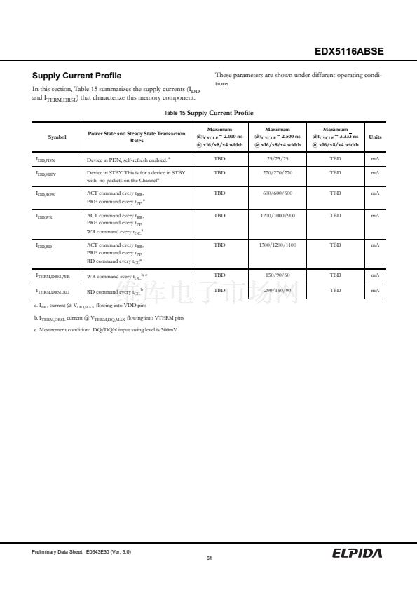
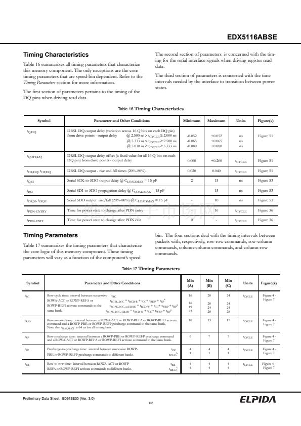
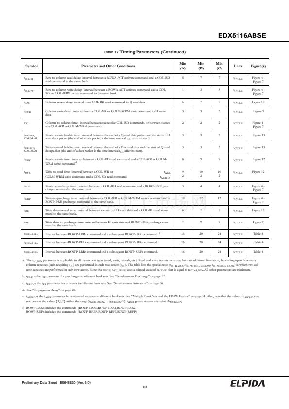
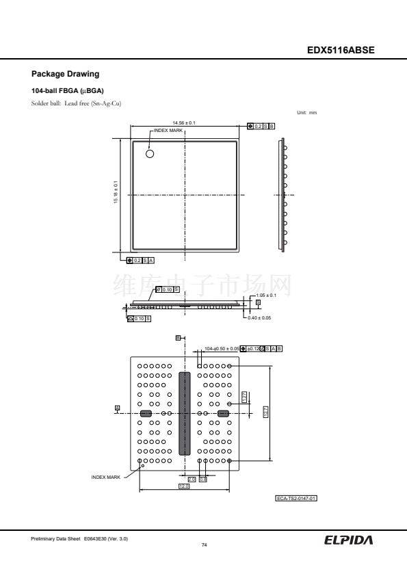
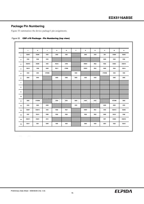
EDX5116ABSE
Special Feature Description
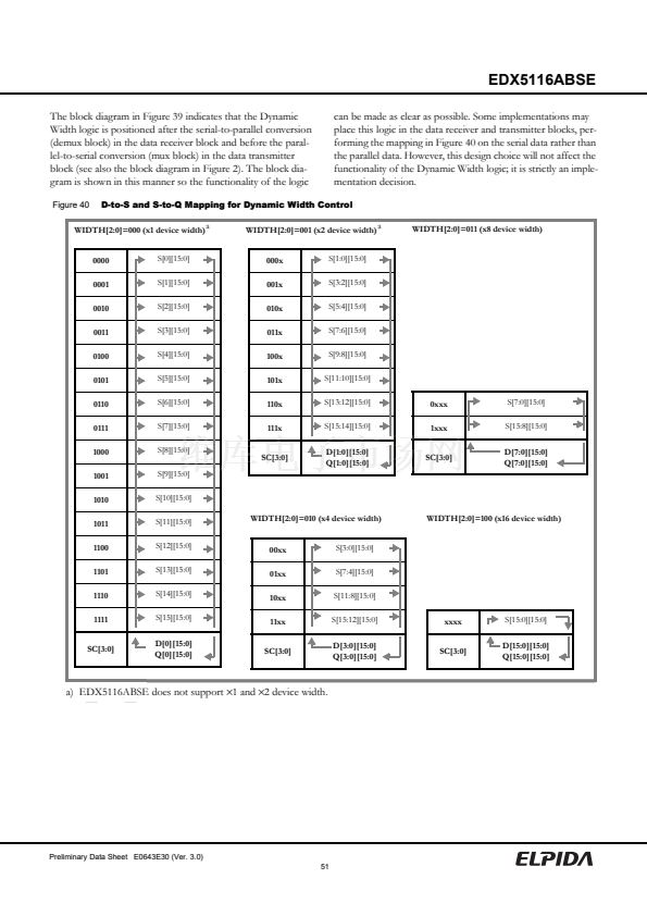
Dynamic Width Control
This XDR DRAM device includes a feature called dynamic
width control. This permits the device to be configured so that
read and write data can be accessed through differing widths of
DQ pins. Figure 39 shows a diagram of the logic in the path of
the read data (Q) and write data (D) that accomplishes this.
The read path is on the right of the figure. There are 16 sets of
S signals (the internal data bus connecting to the sense amps of
the memory core), with 16 signals in each set. When the XDR
DRAM device is configured for maximum width operation
(using the WIDTH[2:0] field in the CFG register), each set of
16 S signals goes to one of the 16 DQ pins (via the
Q[15:0][15:0] read bus) and are driven out in the 16 time slots
for a read data packet.
When the XDR DRAM device is configured for a width that
is less than the maximum, some of the DQ pins are used and
the rest are not used. The SC[3:0] field of the COL request
packets select which S[15:0][15:0] signals are passed to the
Q[15:0][15:0] read bus and driven as read data.
Figure 40 shows the mapping from the S bus to the Q bus as a
function of the WIDTH[2:0] register field and the SC[3:0] field
of the COL request packet. There is a separate table for each
valid value of WIDTH[2:0]. In each table, there is an entry in
the left column for each valid value of SC[3:0]. This field
should be treated as an extension of the C[9:4] column address
field. The right hand column shows which set of S[15:0][15:0]
Figure 39
Multiplexers for Dynamic Width Control
signals are mapped to the Q read data bus for a particular value
of SC[3:0].
For example, assume that the WIDTH[2:0] value is 鈥?10鈥? indi-
cating a device width of x4. Looking at the appropriate table in
Figure 40, it may be seen that in the SC[3:0] field, the SC[1:0]
sub-column address bits are not used. The remaining SC[3:0]
address bit(s) selects one of the 64-bit blocks of S bus signals,
causing them to be driven onto the Q[3:0][15:0] read data bus,
which in turn is driven to the DQ3..0/DQN3..0 data pins. The
Q[15:4][15:0] signals and DQ15..4/DQN15..4 data pins are
not used for a device width of x4.
The write path is shown on the left side of Figure 39. As
before, there are 16 sets of S signals (the internal data bus con-
necting to the sense amps of the memory core), with 16 signals
in each set. When the XDR DRAM device is configured for
maximum width operation (using the WIDTH[2:0] field in the
CFG register), each set of 16 S signals is driven from one of the
16 DQ pins (via the D[15:0][15:0] write bus) from each of the
16 time slots for a write data packet.
Figure 40 also shows the mapping from the D bus to the S bus
as a function of the WIDTH[2:0] register field and the SC[3:0]
field of the COL request packet. There is a separate table for
each valid value of WIDTH[2:0]. In each table, there is an entry
in the left column for each valid value of SC[3:0]. This field
should be treated as an extension of the C[9:4] column address
field. The right hand column shows which set of S[15:0][15:0]
signals are mapped from the D read data bus for a particular
value of SC[3:0].
S[15:0][15:0]
16x16
8
M[7:0]
4+3
WIDTH[2:0]
SC[3:0]
Byte Mask (WR)
16x16
D1[15:0][15:0]
Dynamic Width Mux (RD)
16x16
Q[15:0][15:0]
4+3
WIDTH[2:0]
SC[3:0]
16x16
Dynamic Width Demux (WR)
16x16
D[15:0][15:0]
Preliminary Data Sheet E0643E30 (Ver. 3.0)
50


 1
1
 2
2
 3
3
 4
4
 5
5
 6
6
 7
7
 8
8
 9
9
 10
10
 11
11
 12
12
 13
13
 14
14
 15
15
 16
16
 17
17
 18
18
 19
19
 20
20
 21
21
 22
22
 23
23
 24
24
 25
25
 26
26
 27
27
 28
28
 29
29
 30
30
 31
31
 32
32
 33
33
 34
34
 35
35
 36
36
 37
37
 38
38
 39
39
 40
40
 41
41
 42
42
 43
43
 44
44
 45
45
 46
46
 47
47
 48
48
 49
49
 50
50
 51
51
 52
52
 53
53
 54
54
 55
55
 56
56
 57
57
 58
58
 59
59
 60
60
 61
61
 62
62
 63
63
 64
64
 65
65
 66
66
 67
67
 68
68
 69
69
 70
70
 71
71
 72
72
 73
73
 74
74
 75
75
 76
76
 77
77
 78
78
