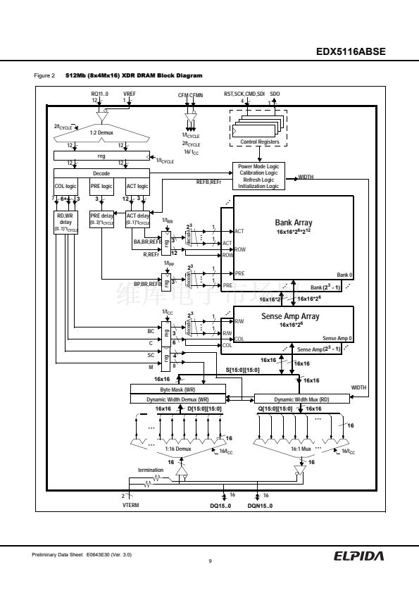
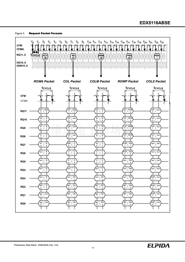
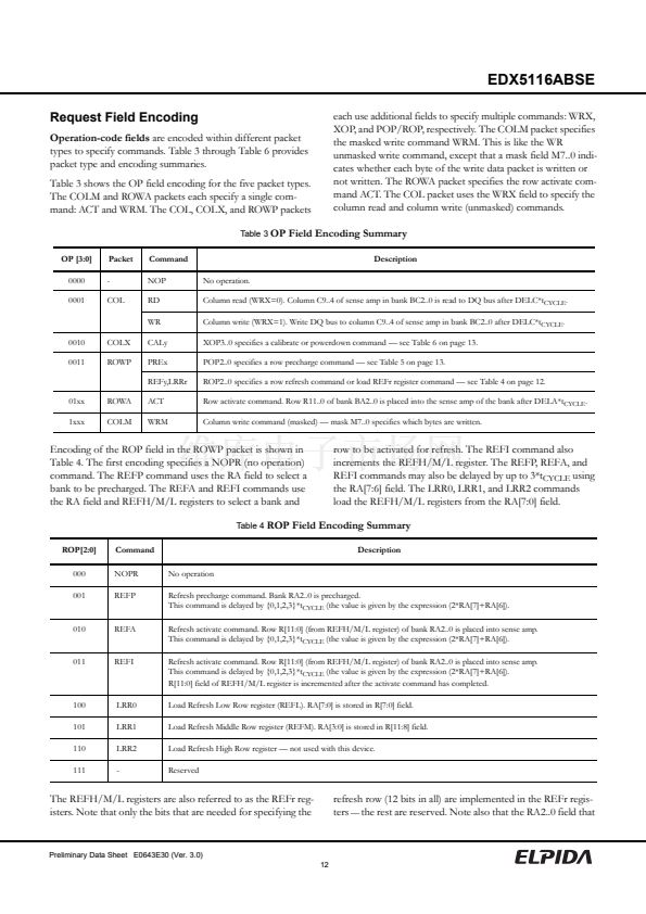
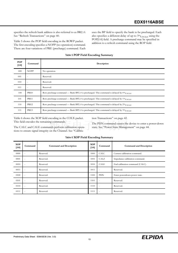
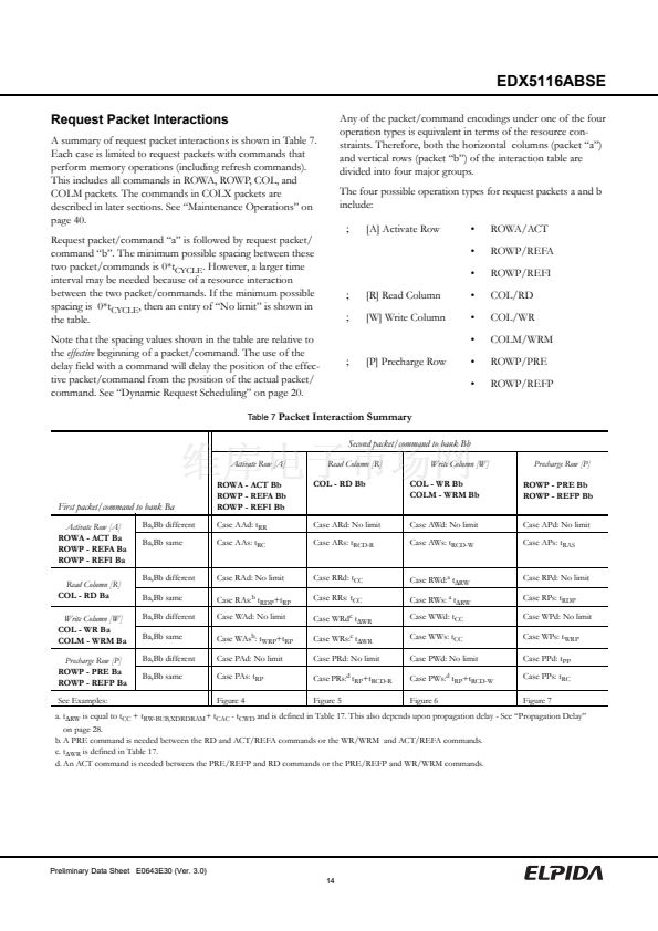
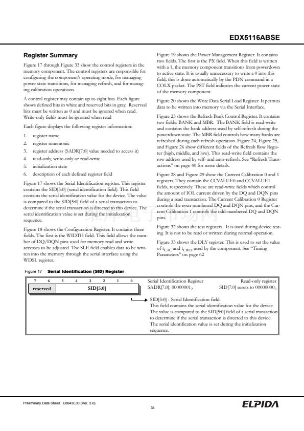
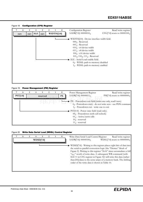
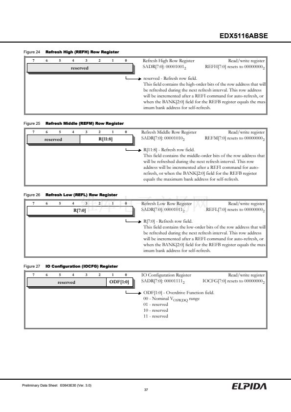
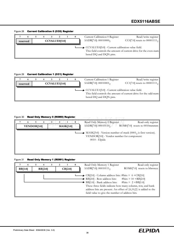
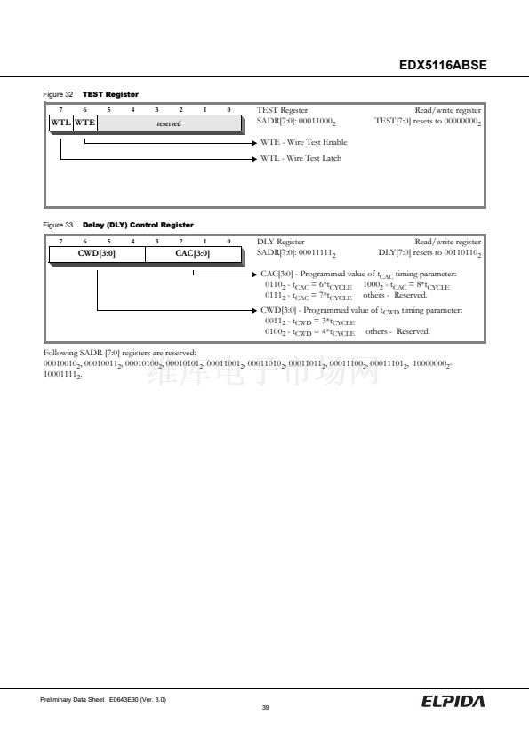
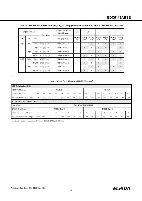
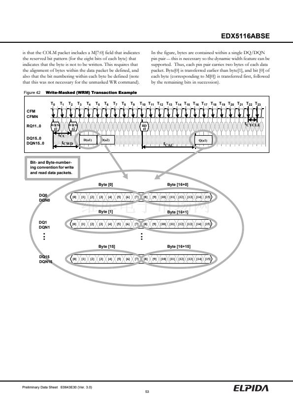
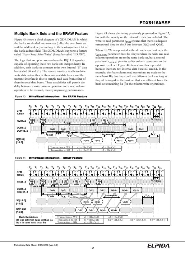
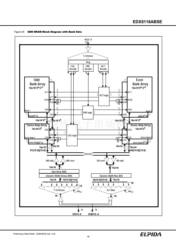
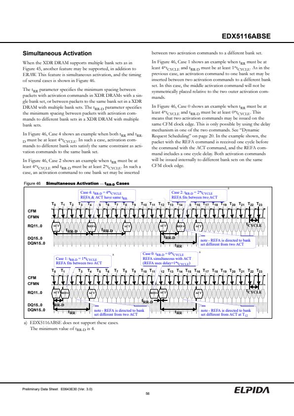
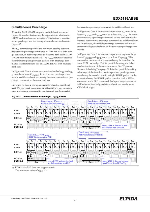
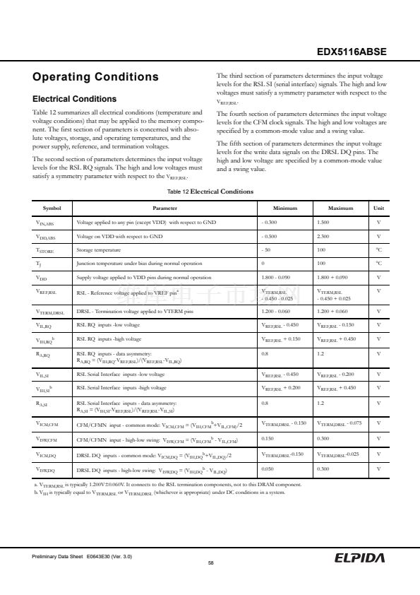
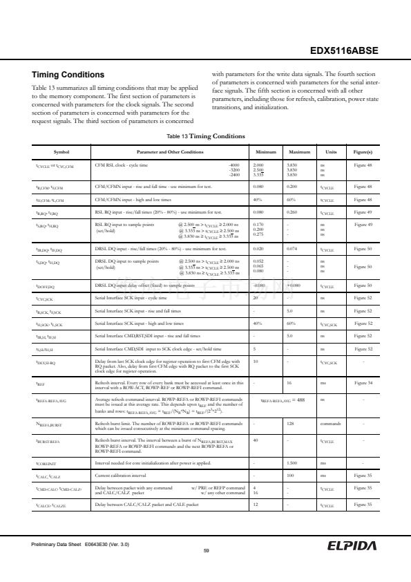
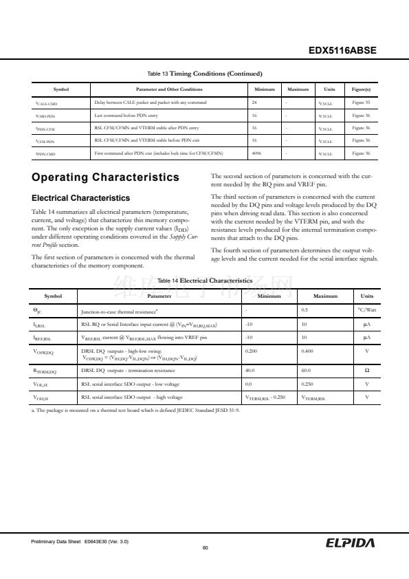
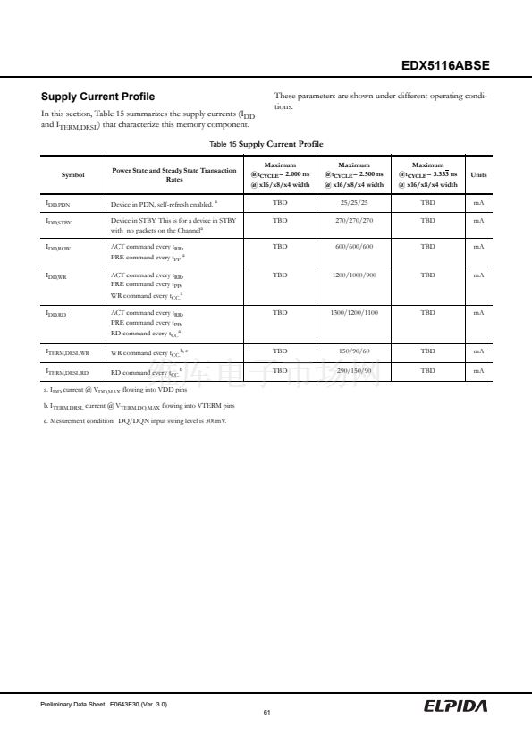
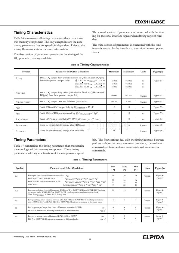
EDX5116ABSE
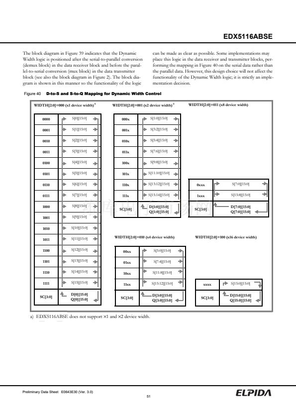
The block diagram in Figure 39 indicates that the Dynamic
Width logic is positioned after the serial-to-parallel conversion
(demux block) in the data receiver block and before the paral-
lel-to-serial conversion (mux block) in the data transmitter
block (see also the block diagram in Figure 2). The block dia-
gram is shown in this manner so the functionality of the logic
Figure 40
can be made as clear as possible. Some implementations may
place this logic in the data receiver and transmitter blocks, per-
forming the mapping in Figure 40 on the serial data rather than
the parallel data. However, this design choice will not affect the
functionality of the Dynamic Width logic; it is strictly an imple-
mentation decision.
D-to-S and S-to-Q Mapping for Dynamic Width Control
WIDTH[2:0]=001 (x2 device width)
a
000x
00x
001x
01x
010x
10x
011x
11x
100x
SC[2:0]
101x
110x
111x
SC[3:0]
S[1:0][15:0]
S[4,0][15:0]
S[3:2][15:0]
S[5,1][15:0]
S[5:4][15:0]
S[6,2][15:0]
S[7:6][15:0]
S[7,3][15:0]
S[9:8][15:0]
D[1:0][15:0]
Q[1:0][15:0]
S[11:10][15:0]
S[13:12][15:0]
S[15:14][15:0]
D[1:0][15:0]
Q[1:0][15:0]
0xxx
1xxx
SC[3:0]
S[7:0][15:0]
S[15:8][15:0]
D[7:0][15:0]
Q[7:0][15:0]
WIDTH[2:0]=011 (x8 device width)
WIDTH[2:0]=000 (x1 device width)
a
0000
000
0001
001
0010
010
0011
011
0100
100
0101
101
0110
110
0111
111
1000
SC[2:0]
1001
S[0][15:0]
S[1][15:0]
S[2][15:0]
S[3][15:0]
S[4][15:0]
S[5][15:0]
S[6][15:0]
S[7][15:0]
S[8][15:0]
D[0][15:0]
Q[0][15:0]
S[9][15:0]
S[10][15:0]
1010
WIDTH[2:0]=010 (x4 device width)
S[11][15:0]
1011
0xx
1100
1xx
1101
SC[2:0]
1110
1111
SC[3:0]
S[6,2,4,0][15:0]
S[12][15:0]
S[7,3,5,1][15:0]
S[13][15:0]
D[3:0][15:0]
S[14][15:0]
Q[3:0][15:0]
S[15][15:0]
D[0][15:0]
Q[0][15:0]
WIDTH[2:0]=011 (x8 device width)
WIDTH[2:0]=010 (x4 device width)
xxx
00xx
SC[2:0]
01xx
10xx
11xx
SC[3:0]
S[7:0][15:0]
S[3:0][15:0]
D[7:0][15:0]
S[7:4][15:0]
Q[7:0][15:0]
S[11:8][15:0]
S[15:12][15:0]
D[3:0][15:0]
Q[3:0][15:0]
WIDTH[2:0]=100 (x16 device width)
xxxx
SC[3:0]
S[15:0][15:0]
D[15:0][15:0]
Q[15:0][15:0]
A16
A8
a) EDX5116ABSE does not support
脳1
and
脳2
device width.
Preliminary Data Sheet E0643E30 (Ver. 3.0)
51


 1
1
 2
2
 3
3
 4
4
 5
5
 6
6
 7
7
 8
8
 9
9
 10
10
 11
11
 12
12
 13
13
 14
14
 15
15
 16
16
 17
17
 18
18
 19
19
 20
20
 21
21
 22
22
 23
23
 24
24
 25
25
 26
26
 27
27
 28
28
 29
29
 30
30
 31
31
 32
32
 33
33
 34
34
 35
35
 36
36
 37
37
 38
38
 39
39
 40
40
 41
41
 42
42
 43
43
 44
44
 45
45
 46
46
 47
47
 48
48
 49
49
 50
50
 51
51
 52
52
 53
53
 54
54
 55
55
 56
56
 57
57
 58
58
 59
59
 60
60
 61
61
 62
62
 63
63
 64
64
 65
65
 66
66
 67
67
 68
68
 69
69
 70
70
 71
71
 72
72
 73
73
 74
74
 75
75
 76
76
 77
77
 78
78
