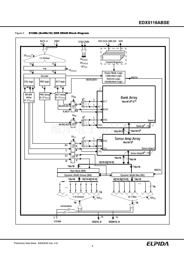
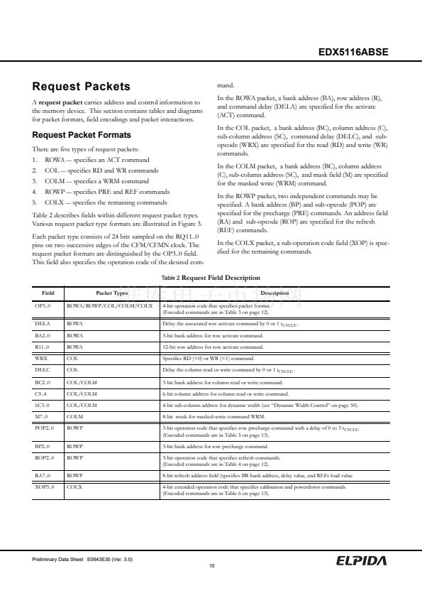
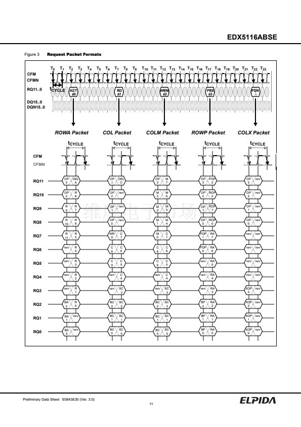
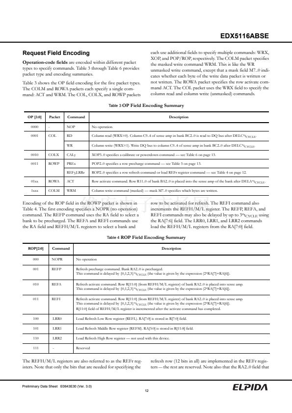
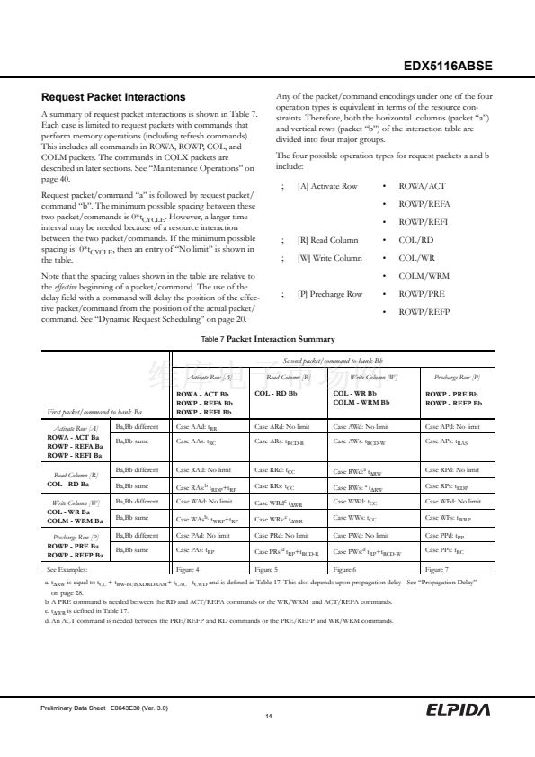
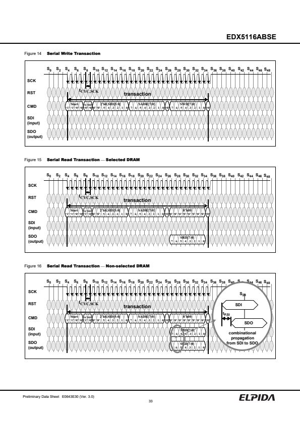
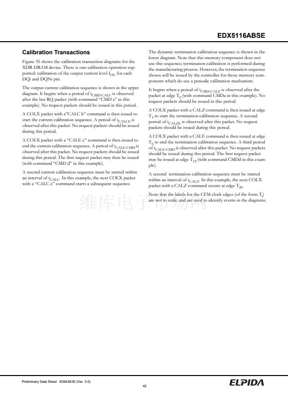
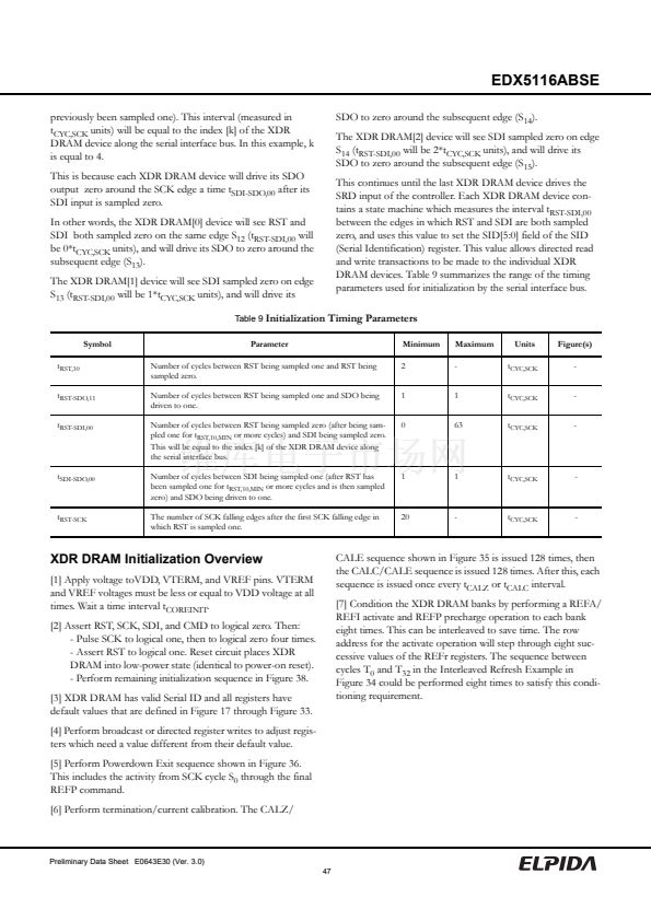
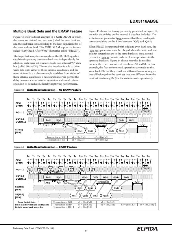
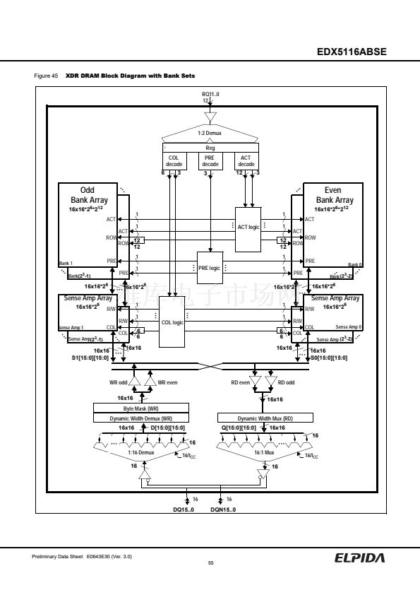
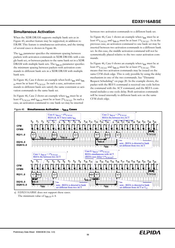
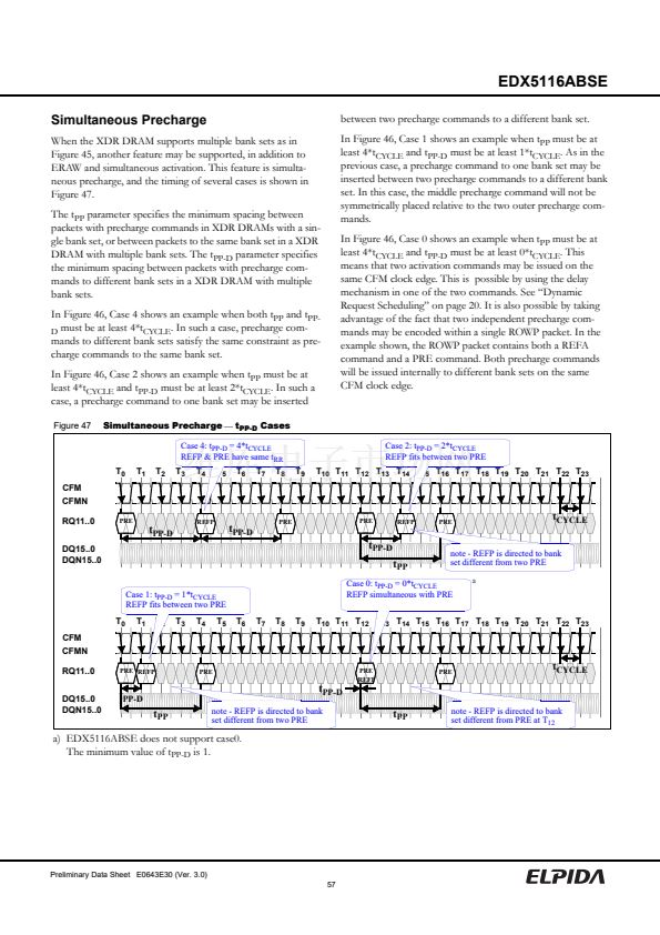
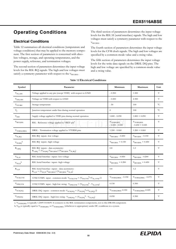
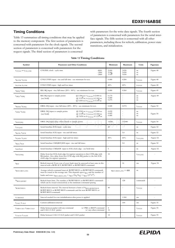
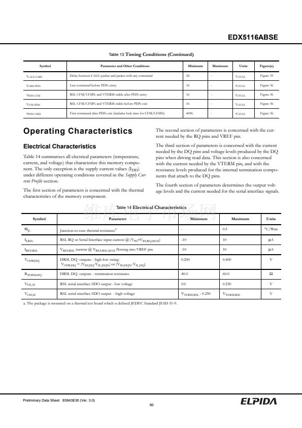
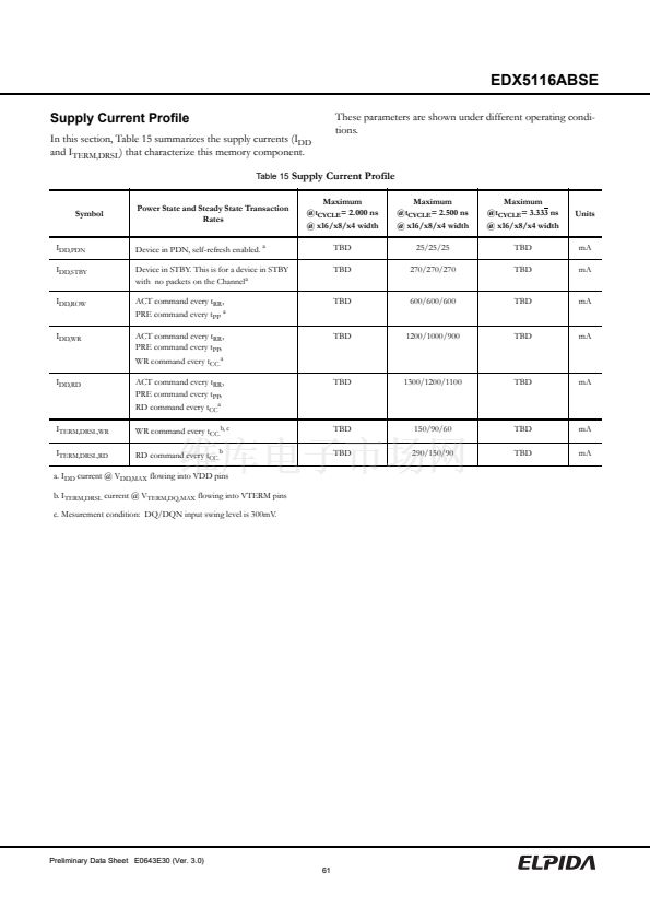
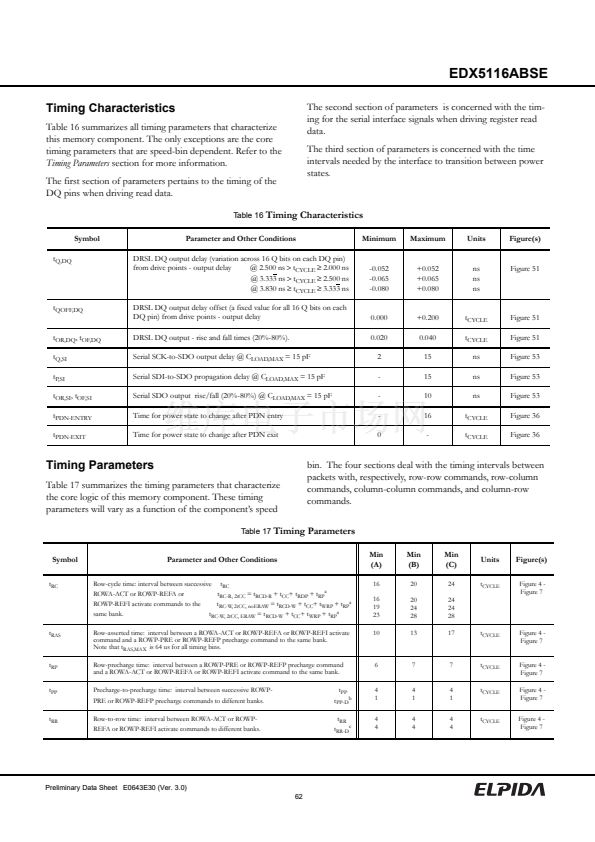
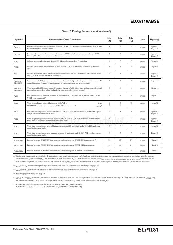
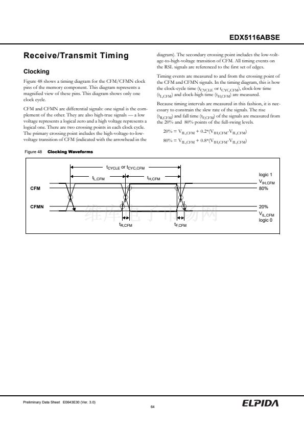
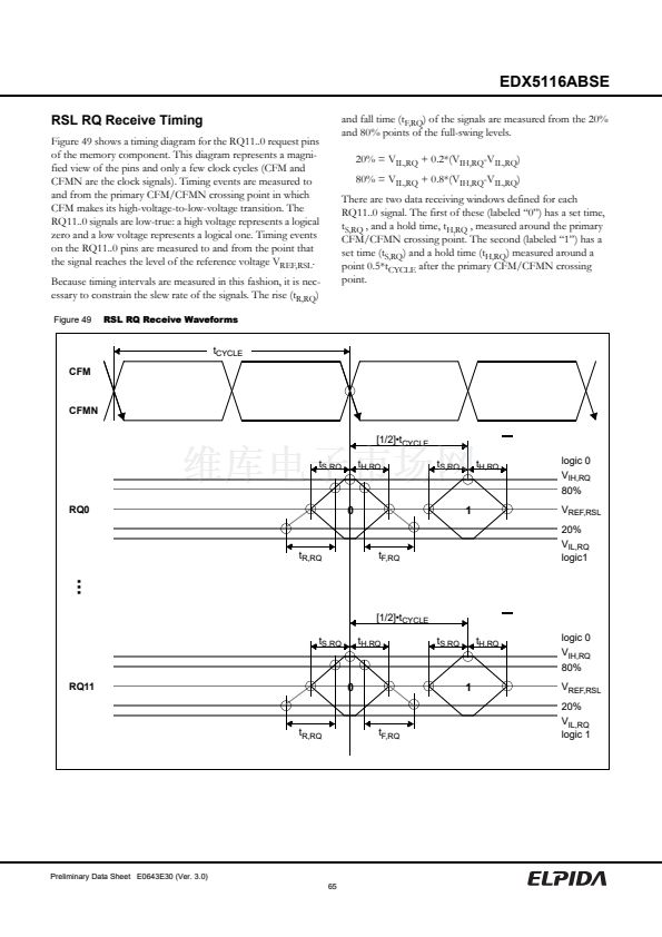
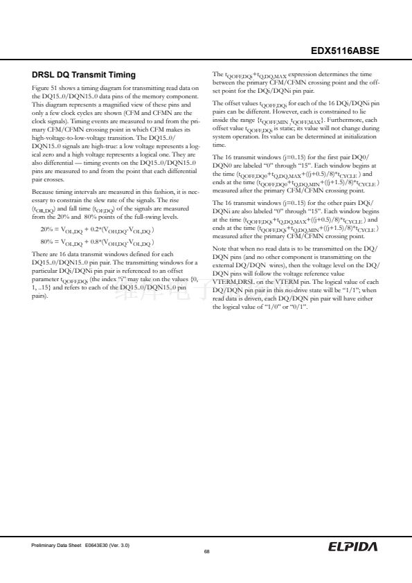
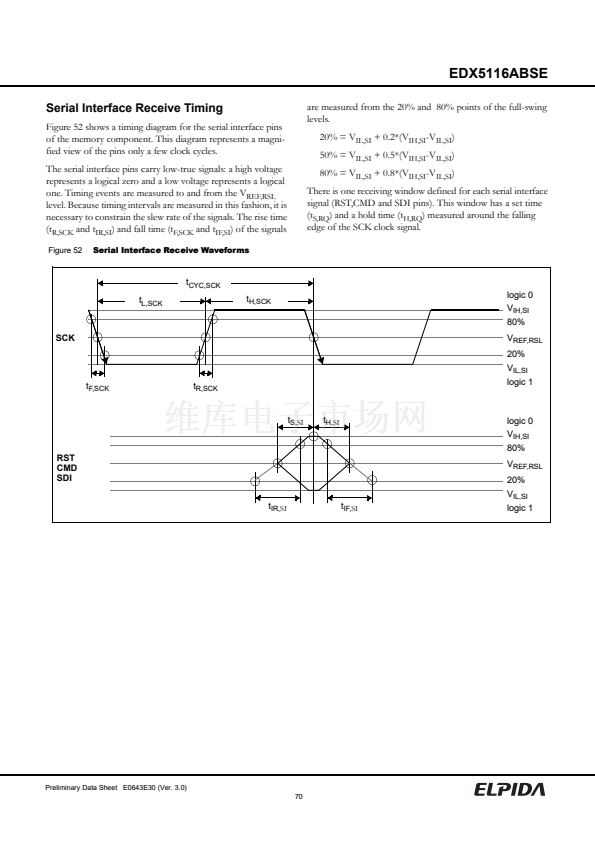
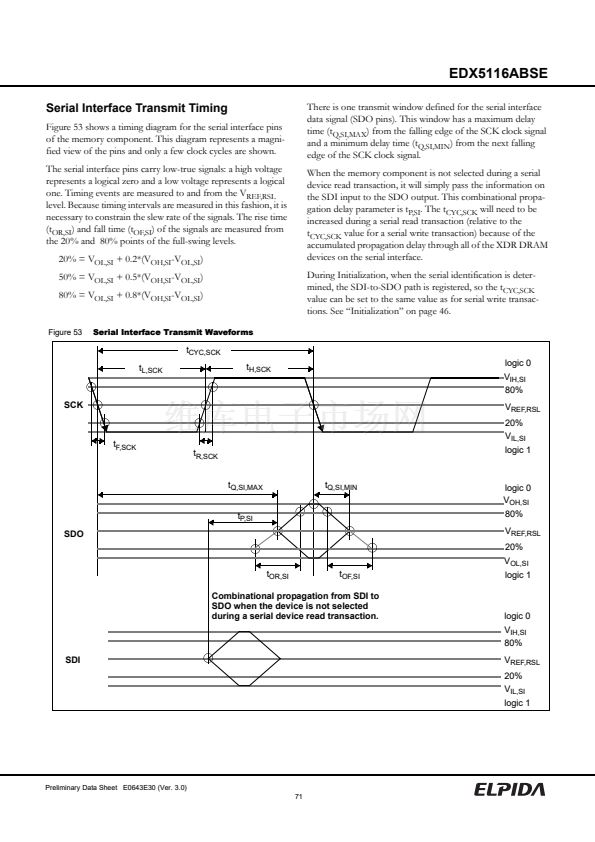
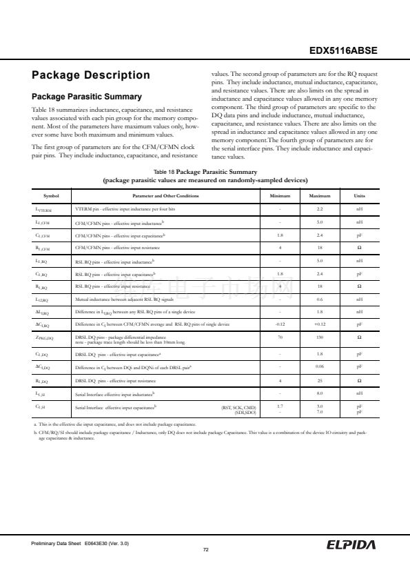
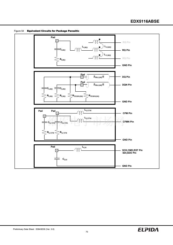
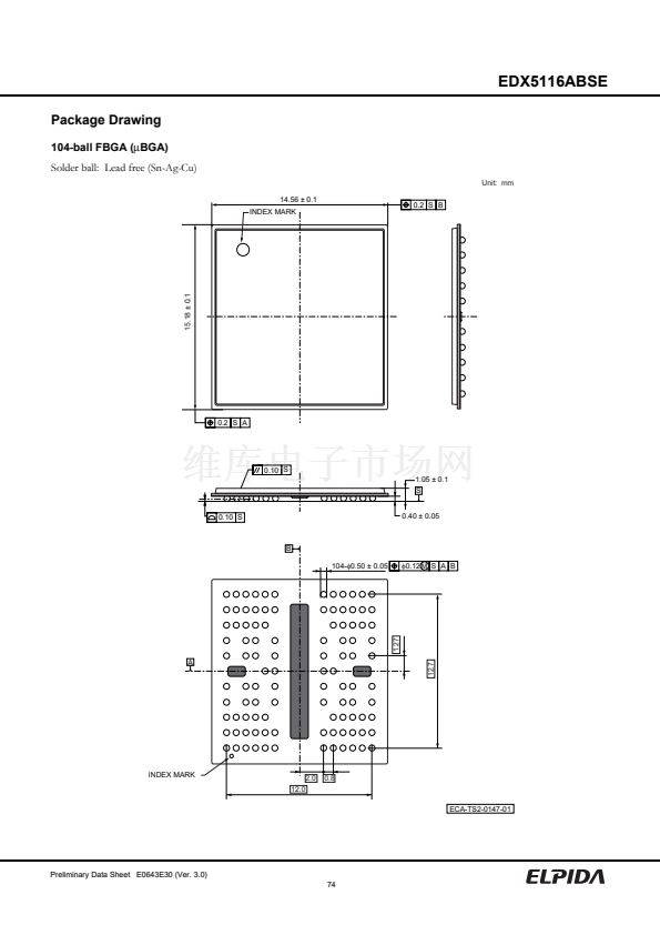
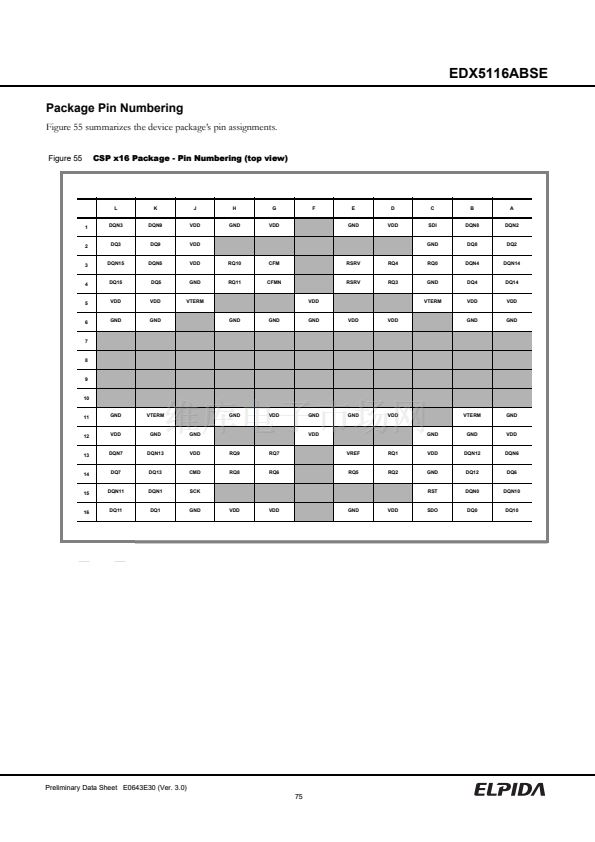
EDX5116ABSE
Write Masking
Figure 41 shows the logic used by the XDR DRAM device
when a write-masked command (WRM) is specified in a
COLM packet. This masking logic permits individual bytes of a
write data packet to be written or not written according to the
value of an eight bit write mask M[7:0].
In Figure 41, there are 16 sets of 16 bit signals forming the
D1[15:0][15:0] input bus for the Byte Mask block. These are
treated as 2x16 8-bit bytes:
D1[15][15:8]
D1[15][7:0]
...
D1[1][15:8]
D1[1][7:0]
D1[0][15:8]
Figure 41
Byte Mask Logic
S[15][7:0]
WE-MSB
[15]
1
NE
Compare
8
8
D1[15][15:8]
D1[0][7:0]
The eight bits of each byte is compared to the value in the byte
mask field (M[7:0]). If they are not equal (NE), then the corre-
sponding write enable signal (WE) is asserted and the byte is
written into the sense amplifier. If they are equal, then the cor-
responding write enable signal (WE) is deasserted and the byte
is not written into the sense amplifier.
In the example of Figure 41, a WRM command performs a
masked write of a 64 byte data packet to all the memory
devices connected to the RQ bus (and receiving the com-
mand). It is the job of the memory controller to search the 64
bytes to find an eight bit data value that is not used and place it
into the M[7:0] field. This will always be possible because there
are 256 possible 8-bit values and there are only 64 possible val-
ues used in the bytes in the data packet.
S[15][15:8]
S[0][15:8]
WE-LSB
[15]
1
NE
Compare
8
8
WE-MSB
[0]
1
NE
Compare
8
8
D1[0][15:8]
8
D1[0][15:8]
S[0][7:0]
WE-LSB
[0]
1
NE
Compare
8
8
D1[0][7:0]
8
D1[0][7:0]
8
8
8
8
8
8
8
8
M[7:0]
8
D1[15][7:0]
8
D1[15][7:0]
D1[15][15:8]
S[15:0][15:0]
16x16
8
M[7:0]
4+3
WIDTH[2:0]
SC[3:0]
Byte Mask (WR)
16x16
D1[15:0][15:0]
Dynamic Width Mux (RD)
16x16
Q[15:0][15:0]
4+3
WIDTH[2:0]
SC[3:0]
16x16
Dynamic Width Demux (WR)
16x16
D[15:0][15:0]
Note that other systems might use a data transfer size that is
different than the 64 bytes per t
CC
interval per RQ bus that is
used in the example in Figure 41.
Figure 42 shows the timing of two successive WRM com-
mands in COLM packets. The timing is identical to that of two
successive WR commands in COL packets. The one difference
Preliminary Data Sheet E0643E30 (Ver. 3.0)
52


 1
1
 2
2
 3
3
 4
4
 5
5
 6
6
 7
7
 8
8
 9
9
 10
10
 11
11
 12
12
 13
13
 14
14
 15
15
 16
16
 17
17
 18
18
 19
19
 20
20
 21
21
 22
22
 23
23
 24
24
 25
25
 26
26
 27
27
 28
28
 29
29
 30
30
 31
31
 32
32
 33
33
 34
34
 35
35
 36
36
 37
37
 38
38
 39
39
 40
40
 41
41
 42
42
 43
43
 44
44
 45
45
 46
46
 47
47
 48
48
 49
49
 50
50
 51
51
 52
52
 53
53
 54
54
 55
55
 56
56
 57
57
 58
58
 59
59
 60
60
 61
61
 62
62
 63
63
 64
64
 65
65
 66
66
 67
67
 68
68
 69
69
 70
70
 71
71
 72
72
 73
73
 74
74
 75
75
 76
76
 77
77
 78
78
